Board A routed, DRC / ERC / netlist clean7 decisions open · 4 of 14 proposed changes applied
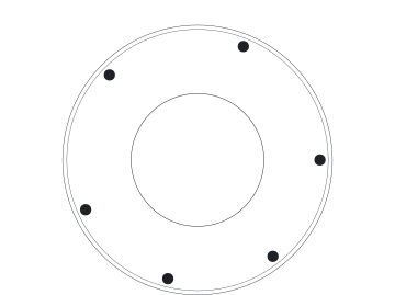
A round, motor-mounted servodrive. Two Ø65 mm boards stacked on the
back of a brushless motor, with the magnetic rotary encoder on the shaft axis: a motor board
carrying the encoder, the three-phase bridge and an RP2350A, and a power/IO board above it.
60 V bus on 80 V silicon, and down to 12 V.
The dot puts a layer on top at full
opacity; the box says whether it is drawn at all.
1.0×
Keys: 1–9 pick a layer, s solo,
a all, m mirror, 0 fit. Click a part for its pane;
coordinates are pcbnew’s, in millimetres.
The model loads when this tab is open.
Board A
The power board of the two-board servodrive: three phase cells, the RP2350A and the MT6701 encoder on a Ø65 mm six-layer board that bolts to the back of the motor.
Source
hardware/motor_board/servodrive_A.kicad_pcb
Board
Ø65 mm6 copper layers, 1.6 mm thick
Parts
140 footprints82 on the front, 58 on the back
Copper
87 nets, 1,361 track segments, 278 vias2,062 mm of routed track
3D
120 of 140 parts drawn from a model3 through an older KiCad’s library variable (${KICAD6_3DMODEL_DIR} and so on), read as KiCad 9’s libraryL701 with a stand-in from the project file20 name no model (H1–H4, H10–H15, J1–J3, TL1–TL3, TP1–TP4)
Built 2026-10-03 00:11 by pcbview from the KiCad files above:
python3 -m pcbview build pcbview.toml. Nothing here is drawn by hand — the layer plots, the model and the
sheets are KiCad’s own exports.
Copper, layer by layer
Board A's six copper layers as routed, plotted straight out of the board file by KiCad
and stacked in register. Pick a layer to bring it to the front; drag to pan, scroll to zoom
— they are vector, so a 0.15 mm track stays a track all the way in. Click a part for
its pane. The cursor reads out pcbnew's x and y, and the radius and angle the floorplan is
written in, so a run can be checked against the numbers in tools/geometry.py
without leaving the page: angles are measured from the +x axis, the way the section
boundaries at 0/68/136/204/256/308° are.
The viewer is pcbview's (configured by
pcbview.toml); gen_boards.py and route.py rebuild it
through tools/regen.py, or by hand python3 tools/regen.py --board a.
Drill holes are painted in the plate colour, so a hole reads as a hole on every layer; the
outline layer carries all of them and sits on top.
The board in 3D
Board A as routed, every part that has a model standing on it, exported through KiCad's
own GLB exporter. Drag to turn it over, right-drag to pan, scroll to zoom. Hover a part for
its reference, value and footprint; click it for the pane on the right — what it is for,
where it sits, how tall it stands, and the net on every pin. Double-click or type a reference
to fly to it. Turn off the mask to see the copper under it, the laminate to see both faces'
copper at once; the edge view shows how tall each face stands.
Board A is placed, captured and routed, and every connection is made.
136 parts, 87 nets, 425 pin connections; 1361 track segments and 278 vias. DRC finds
nothing, ERC finds nothing, nothing is unconnected, no right-angle corners survive, and
KiCad's own exported netlist matches the one the repo intended — net by net,
connection by connection. The whole board comes out of
tools/gen_boards.py, so the drawings, the floorplan and the netlist cannot
drift from the numbers the spec quotes.
Re-routed 2026-09-22 with four of the simulation's changes, and five
open questions answered: XT30 for the bus, a reset brakes, SimpleFOC, VMOT down to
12 V, and no enclosure fins — 20 A is a burst to be measured on the
prototype, not a continuous rating. On the board: every barrel under the low-side drains now
reaches the switch-node pour on B.Cu (four of sixteen did), the high sides have twenty
barrels rather than sixteen, each cell carries an unfitted RC snubber, the LIN pulls go to
GND, and the magnet is Ø6. The simulation's conduction solver, re-run on the routed
board, has the busiest low-side barrel at 2.82 A rms (was 5.16) and
the busiest high-side one at 2.10 (was 2.42): better, and still over the
2 A guideline at a continuous 20 A; under it below about 14 A RMS.
The simulation — ten phases, fourteen questions, twenty-four
findings (the report) — still describes the board
before those changes; sim/results/ was not re-run into place. Its
other two corrections to the design's arithmetic are not applied yet: the commutation loop
is about 2 nH where geometry.commutation_loop() says
0.39, and the DC-link ceramics are worth about half their marking at 60 V.
What is not done: nobody has looked at board A's routing by eye, and
board B is still an outline — now with three things waiting for it: the gate rail's
enable held on through a reset, and the polymer-hybrid bulk. (USB-PD and a pack on the XT30
are not used together, so the PD front end stays as specified.)
Open decisions — waiting on a person
How hard does the EG2103's output stage actually drive? The only
obtainable document gives IO+/IO− with no test condition, and
the whole edge hangs off it: 62.6 V of Vds with no ring and no snubber at
the datasheet reading, 73.9 V and a 145 MHz ring at a strong output stage. It
decides Q2, Q3, Q4 and Q12 between them. Get the real datasheet, or measure the gate edge
into a known capacitance on a built board.
Which motor? Sets the air gap, the standoffs, and whether the
25 × 19 mm pattern bolts to anything. Deliberately deferred —
one constant in geometry.py moves the whole stack.
What happens on a decel? At the design-point braking torque the bus
reaches the TVS breakdown in 0.26 ms and leaves about 2 J on a part that
survives a few. There is no brake chopper; the firmware's 63–66 V fold-back
reacts in one 50 µs period. A brake resistor, an active clamp, much more bulk,
or a documented deceleration limit. (A reset now brakes, which does not pump the
bus; a controlled decel still does.)
How is the motor frame bonded? Nothing on this board bonds it
— the four motor mounts are NPTH — so it follows the switch node to
71 V peak against a 10 V criterion, and a long bonding wire makes it worse,
not better. The sweep's best option is a 4.7 nF Y capacitor at 2 V of frame
swing. Measure the motor's winding-to-frame capacitance first; the table moves with it.
E-stop loop: keep it?
Hardware overcurrent trip: populate, DNP, or omit.
Interconnect — header, or brass standoffs as the power path.
Full text in §11 of the spec; 1, 3 and 4
come out of the simulation's own open findings. Decided 2026-09-22 and taken off this list:
XT30 for the bus, a reset brakes, SimpleFOC, VMOT down to 12 V, no enclosure fins, and
USB-PD as a replacement for a pack rather than alongside one.
Changes the simulation proposes
Fourteen of them; the four at the top were applied on 2026-09-22 with one re-route.
sim/ does not touch hardware/ or tools/; this is the
hand-back list, for a human to decide from, and its own register still lists all fourteen
because it has not been re-run into place.
Change
Where
What it buys
Cost to apply
Widen the SW_x pour on B.Cu to cover the whole 4 × 4 array, or move the
array inboard of the PHASE pour
tools/gen_boards.py: via_tab()
Twelve of sixteen barrels stop being islands. Measured after: all sixteen joined, the
busiest at 2.82 A rms from 5.16 — not the four times hoped for, because the
current crowds toward the shunts
applied 2026-09-22
More VBUS vias under the high-side drains, or spread the entry into the array
geometry.py: FET_VIA_NY_HS (5 rows, 20 barrels)
The busiest high-side via carried 2.4 A rms against 2 A. Measured after:
2.10. A fifth row is all that fits
applied 2026-09-22
Two unstuffed 0805 per cell for an RC snubber, 2.2 Ω + 0.47 nF,
SW_x to GND
Worst Vds 73.9 → 62.7 V for 0.034 W per cell, if
the driver turns out to be the strong one. Placed as 0603, which is what fits
applied 2026-09-22, DNP
Magnet Dia 6 × 2.5 mm, as the MT6701 datasheet recommends, or
an N35 with the gap held at or above 1 mm
geometry.py: MAGNET_D (6.0)
Keeps the field at the die inside the part's 20–100 mT window over the
whole air-gap tolerance; Ø8 was over 100 mT at the short end. The price,
measured 2026-09-22 (P5S): the weaker field lets the motor leads move the angle
further, 0.12° at the nominal 1.5 mm gap where P5 had 0.09° — which makes
the lead-twisting row below matter more
applied 2026-09-22 — no board geometry reads it
Commutation loop 1.98 nH — the solved value at the converged end of its own
grid sweep — not µ0hl/w = 0.387
geometry.py: commutation_loop()
Every number derived from it moves: overshoot, ring frequency, the snubber decision
a number only
DC-link ceramics 7.0 µF at 60 V (bracket 5.5–9.7), not 13.2
geometry.py: interconnect()
The ripple split shifts and more of it crosses the header
a number only
Budget Miller cross-conduction — 0.86 W per half-bridge and a 74 A peak
— or pick a device with a smaller Qgd/Ciss
geometry.py switching-loss term, or the FET choice
The off device's Vgs reaches 3.62 V at the die on every high-side
turn-on, above its own 2.2 V minimum threshold. Neither Rg, a stronger
driver, nor a gate-source capacitor moves it
a number only, unless the device changes
Board B bulk: 4 × 100 µF polymer hybrid at
20–40 mΩ each, not 3 × 100 µF electrolytic
at 0.2 Ω
spec.html §8
Bus ripple at the drains falls from over 6 V p-p to under 2
board B, not yet captured
Pace the ADC from the PWM slice's wrap DREQ — one conversion per phase at the
counter's zero, instead of free-running round-robin
Current-loop measurement error 0.638 → 0.210 A rms, and the bias
halves
firmware
Set dead_zone to 0 and rely on the EG2103's own 560 ns interlock
firmware
Recovers 0.76 % of torque and changes the distortion hardly at all
firmware
Clamp the modulation index: never command a duty below 2.40 % or above its mirror
firmware
Keeps the loop out of the region where the driver's minimum pulse silently passes
nothing
firmware
Twist or bundle the three phase leads for the first 50 mm after the lead pads
assembly instruction, not a board change
Removes most of the 0.090° current-dependent angle error; the board copper's own
field already cancels on the shaft axis
assembly
Give add_barrel() a bar of the plated tube's geometric mean distance, with
conductivity scaled to keep the copper area, then re-run P1 Q1
sim/fasthenry/mesher.py
An equal-area bar is right for R and 2.2× too inductive for a
0.4 mm drill, and the loop runs through sixteen of them
the simulation's own model
Known-answer expectation 14.53 nH, not 17.4, for the straight wire at
l = 20 mm, d = 1 mm
sim/SPEC.md §5.4
The test passes as written once the expected value is right; FastHenry already returns
the formula's own answer to 0.03 %
a number only
Each row's evidence, and the six findings still marked OPEN rather than
HAND-BACK, are in the report;
sim/FINDINGS.md is the register and sim/HANDBACK.md the list as
generated. Cite a finding by its evidence key — the S-numbers are positions in a
severity-sorted table and renumber whenever one is added.
Before ordering
Look at board A's routing by eye. The tools prove DRC, connectivity
and the heatsink land; they do not judge whether a run is where a person would put it
Take the four placement changes above, re-route, and verify again from
scratch — done 2026-09-22
Capture board B: the polymer-hybrid bulk rather than the spec's original
3 × 100 µF, the gate rail's enable pulled on so a
reset brakes
Re-run the simulation (sim/run.py) on the new board, so its register
describes the board that exists
Every placed part has an LCSC number (hardware/parts/lcsc.csv),
INA241A3 included — 2026-09-24. No 1.6 mΩ 2010 is stocked,
so the shunts are 2 × 2 mΩ; the flash is W25Q16JVUXIQ
Past work
Board A, at a glance — the settled numbers
Form
Two Ø65 mm round boards; motor board bolts to the encoder's
4 × M3 pattern, power/IO board to six perimeter M2.5
Sections
Three 68° phase cells adjacent over 0–204°, then three
52° utility wedges. Six M2.5 on the section boundaries, at
0/68/136/204/256/308°
Encoder
MT6701 on the shaft axis, SSI to the CPU on the same board — no
cable, no line drivers, no encoder port
Heat
279 mm² of bare copper laid out for an aluminium ring. No fins:
the drive runs below its peak current, and bursts are measured on the prototype
Bus
60 V nominal, 12 V minimum, 80 V silicon, TVS breakdown 71–79 V; XT30
Phase current
20 A RMS per phase, a burst figure — 28.3 A peak,
±32 A of sense, 10.7 W if it were continuous
CPU
RP2350A, QFN-60. Three PWM slices for three half-bridges; four ADC
channels, all spoken for
Sensing
Two inline 1.0 mΩ shunts (2 × 2 mΩ) + INA241A3 at
50 V/V = 50 mV/A → ±29.0 A, third phase reconstructed; bus voltage; FET
temperature
Gate drive
EG2103 on a 12 V rail — not the sister board's EG3113
at 5 V, for two separate reasons. Six 4.7 k input pulls, which two errata made
compulsory, all to GND: a reset brakes. RC snubber footprints, DNP
I/O
USB-C with full PD — a 20 V contract feeds VMOT and runs the motor —
and full-duplex RS-485 on two chained ports
How it got here — placement, capture, routing
The first routed board made 69 of 170 connections and blamed the driver ring. Measuring it
said otherwise: nearly every open connection ended at the RP2350, which had no room to fan
out. The second pass rebuilt the CPU wedge around a clear band for a four-row escape, turned
the FETs so their gates face the driver row, rearranged the sense row for arcs, and took the
regulator cluster from Raspberry Pi's reference design. Then the connections freerouting does
badly — the QFN escape, the gates, the sense nets — were made as copper by a tool before the
router ran. The last three connections turned out to be arithmetic rather than routing: the
escape via rows were 0.71 mm apart and a track passing between two of them needs 0.91, so
there was no radial lane out of the via field at all. Moving the outermost row out 0.2 mm
bought one, and freerouting finished the board in its first round. §10 and §10b of
the spec have the detail.
The phase cells are 68°, not the 60 the floorplan sweep promised.
Routing found that the channel interior to the screws can only hold parts whose nets are
ground or the phase output, so five per cell came back in and the cells had to pay for them.
It costs the even bolt circle and buys 29 mm² of heatsink land.
The three phase cells are adjacent rather than alternating with the
utility wedges — the RP2350A sits in the middle of the quiet side instead of between two
switching cells, and the three motor leads leave together.
Three things unblocked the specification itself. The drive is rated 20 A RMS per
phase, continuous, which settles the thermal question by paying for it. The EG2103
datasheet was read rather than argued about. And the motor is set aside — every dimension
that depends on it is derived from one constant in geometry.py, so naming the
motor later moves the whole stack at once.
Committing to 20 A found two real errors in draft 0.2. Capturing the schematic found
seven more — the RP2350A had no core-buck inductor, the bus divider would have put 5.5 V on
a 3.3 V ADC pin, and the MOSFET's symbol and footprint numbered their pins differently,
which would have wired every FET backwards. That is what capture is for.
What is settled
Ø65 mm, both boards
60 V bus, 12 V minimum, 80 V silicon; 20 A RMS in bursts,
not continuous — no fins (2026-09-22)
XT30 bus input; SimpleFOC firmware; a reset brakes (2026-09-22)
Board-side thermal path: 279 mm² of bare copper for an aluminium ring
Sense chain resized to reach the design point's 28.3 A peak — twice
Three phase cells grouped adjacent, 68° each, bolts at
0/68/136/204/256/308°
Board A captured: 136 components, 87 nets, ERC clean
Board A routed: all 425 connections, DRC clean, heatsink land clear
RP2350 regulator cluster and 1V1 ring from the RP-006440 reference design
EG2103's LIN is pulled up inside the part — read off the datasheet,
not argued; the board pulls it down, so a reset brakes
Six 4.7 k input pulls, because RP2350-E9 meets that pull-up
Board A floorplan: 98 parts, DRC- and ERC-clean
USB-C with PD (20 V to VMOT) + full-duplex RS-485, two ports, chained
Encoder circuit and mount pattern inherited from the sister project
12 V gate rail with EG2103 — closes two of their open findings
Interlock + 560 ns hardware dead time kept, at ~2 W of edge rate
The sense chain's DC accuracy, measured: 0.8301 mΩ tap to tap,
3.6 % of it copper, 0.019 %/K total TCR
No gate-source capacitors: 22 nF moves the pin and not the die, because
1.6 Ω of internal gate resistance sits between them
The two decisions worth arguing about
The 12 V gate rail is the whole thermal budget. The sister board drives
10 V-rated MOSFETs from a 5.04 V rail, which its own review costs at ~2 W per bridge of
switching loss plus ~15% on RDS(on) (its F-41). It cannot easily fix this,
because thirteen 5.5 V-max analog switches sit on that same rail. This board has no
such rail and no such constraint. Taking the 12 V rail — and with it a driver that wants
one — moves board A from ~18 W to 10.7 W at 20 A RMS. It also shapes the USB-PD behaviour: the
gate rail's buck cannot boost, so before a PD contract is negotiated VMOT sits at 5 V, the
logic and encoder are up and the motor physically cannot energise. Ask for 20 V and it runs.
20 A continuous is a rating the enclosure grants, not one the board has.
Board A is sealed between the motor and board B; neither face sees moving air. Bare, the
stack is about 15 K/W to ambient, and 10.7 W through that puts the junctions at
214 °C. The design is the machined aluminium ring: it clamps
279 mm² of mask-free copper across the three phase cells, bolts through all six
perimeter M2.5 — now plated, padded on every layer, and doubling as the ground bond — and
the whole board is laid out around it, with every outward-face part stopping at
R 29.2. What is left is the outside of that ring: ≥ 100 cm² of
external surface for ≤ 6.7 K/W. A plain Ø65 × 35 mm barrel
is 71 cm² and misses; the same barrel with sixteen 6 mm fins is ~138 cm² and
lands at 105 °C junction. The fins are the rating.
“20 A” meant two different things, and the sense chain lost —
twice.
The thermal budget was written at 20 A RMS per phase; the sense chain was designed
for ±20.6 A instantaneous, to reproduce the sister board's 80 mV/A so its
firmware constants would carry across. Those differ by √2 — the chain would have
clipped on every cycle above 14.6 A RMS, and you cannot close a current loop on a clipped
measurement. The first correction, 1.0 mΩ for ±32 A, was sized against the
amplifier's typical output swing; the datasheet's worst case turns that into
±29 A, which is 2.5% over the peak and not margin. The shunt became
0.8 mΩ (2 × 1.6 mΩ), 40 mV/A, ±36.2 A worst case — 28% clear. And
the part number was wrong too: the 50 V/V grade of INA241 is A3, not A2.
Then sourcing undid it (2026-09-24): no 1.6 mΩ 2010 is stocked at
LCSC or JLCPCB, and the pair is 2 × 2 mΩ — 1.0 mΩ, 50 mV/A,
±29.0 A, the 2.5% again, taken knowingly.
How the hardware is generated
Two KiCad 9 projects, both DRC- and ERC-clean, emitted from
tools/geometry.py, tools/placement.py and
tools/schematic.py by tools/gen_boards.py — so the outlines, the
mount patterns, the thermal land, every part position and every net come from the
same numbers the spec quotes. Board A carries 136 parts and 87 nets; board B is still an
outline. The three tools are checked against each other before anything is written: a part
cannot be on the board and not in the netlist, or the other way round, and their footprints
have to agree.
The schematic is generated and drawn with labels rather than wires — an honest
description of a machine-laid-out sheet. What it is for is a netlist that cannot drift from
the placement, and KiCad's own export confirms it net by net.
hardware/power_board/ — 4 layer, 2 oz outer. Same six M2.5 at
R = 29.5, so the stack aligns. Board A is in the copper viewer at the top of
this page.
Origin
Board centre = the shaft axis = the MT6701 sensing centre, on both
boards. Grid and drill origins set there too.
Symbols
RP2350A QFN-60 lifted from rp2350-bike-light, MT6701
from the sister project's encoder — both copied into
hardware/parts/servodrive.kicad_sym so the projects open standalone.
Design rules
0.15 mm track and clearance — JLCPCB's floor for 2 oz
outer copper — except the 60 V nets at 0.4 mm; vias 0.5/0.20 signal, 0.6/0.30
power, 0.8/0.40 phase; and 0.5 mm hole-to-hole, chosen early so
JLCPCB's free via-in-pad on 6 layers stays available. Their F-48 is the cost of
deciding that late.
Net classes
Track widths Default 0.2, Gate 0.35, Analog 0.25, Power 0.5,
Phase 2.0 mm; the Phase class covers PHASE_*, SW_* and
VBUS, and deliberately not GND. They actually reach KiCad now — the
generated project used uvia_* where KiCad 9 wants microvia_*
plus a priority, and silently fell back to a factory 0.2 mm class.
Placement
136 parts on board A, checked by tools/placement.py
before any board is written: courtyards, radial and sector bounds, the perimeter boss
pads, both arc lands, and through-hole pads landing on the opposite face.
Routing
stitch.py (via-in-pad) and fanout.py (the
QFN escape field, gate and sense arcs, In3 links, plane taps) lay deterministic locked
copper; route.py hands the rest to freerouting 2.2.4 and then
finish.py, a maze router over the board's rasterised free space, closes
whatever is still in pieces.
Regenerate with python3 tools/gen_boards.py --force — which
also stitches and fans out — and then python3 tools/route.py --rounds 4 --loose;
--force throws the routing away, and without it the board is kept and only the
drawings are redone. It refuses to write anything at all if the floorplan check fails.
Handed back to the sister project
Their F-17 is right — and draft 0.2 of this spec was wrong to doubt it.
Their E-stop does brake, but not for the reason their register gives: R1,
R2, R21 and R22 are 10 k pull-downs on both EG3113
inputs, and a pulled-down active-low LIN turns the low side on. The driver alone
would coast. Worth telling them the consequence: their bridge hard-shorts the
motor at every power-up, before firmware runs, with no current limit
RP2350-E9 reaches the gate driver. A Bank 0 input can latch near
2.1–2.2 V; against EG Micro's internal 200 k pull-up on LIN that lands the driver input
between VIL and VIH. Their pull-downs happen to defeat it —
anyone copying the circuit without them should size an external pull deliberately
NCP5183DR2G as an answer to F-40 (EG3113
unbuyable, blocking their orders) — and a warning that EG2131, the obvious swap, is out
of stock too
The observation that its F-41 remedy is cheap on a board without
the TS5A3159 rail constraint
Log — 2026-09-07 to 2026-09-12
Five decisions, four of the simulation's changes, one re-route.
Decided: XT30 for the bus; a reset brakes; SimpleFOC; VMOT down to 12 V;
and no enclosure fins — the drive runs below its peak current and 20 A becomes
a burst to measure on the prototype. On board A, the low side's via array is under a tab
of the switch-node pour on B.Cu, so all sixteen barrels carry current rather than four;
the high side has a fifth row of barrels, twenty in all, which is the most the drain pad
and the shunts' courtyards on the back allow; an unfitted 2.2 Ω + 470 pF
snubber sits under each high side; both input pulls of every driver go to GND; and the
magnet is Ø6. Freerouting finished in its first round again: 1361 segments,
278 vias, DRC, ERC and the netlist diff clean.
The simulation's conduction solver, re-run on the routed board in a scratch copy, is
the honest check: the busiest low-side barrel falls from 5.16 to 2.82 A rms and the
busiest high-side one from 2.42 to 2.10, both still over the 2 A guideline at a
continuous 20 A because the current crowds toward the shunts, and both under it
below about 14 A RMS. Two consequences for board B came with the decisions: the
gate rail has to stay on through a reset, or the brake lasts only as long as its
capacitors; and a 20 V PD contract could back-drive a lower-voltage pack, which
is answered by not using the two together — PD replaces a pack.
The electromagnetic simulation, ten phases.sim/
solves the board rather than estimating it: FastHenry on the copper as routed, FastCap
for the sense taps, ngspice for the edges, openEMS full wave as a cross-check, plus the
encoder field and the thermal path. Fourteen questions, twenty-four findings, four
hypotheses — all four confirmed or resolved. Three answers change the design's own
arithmetic: the commutation loop is 2.06 nH where
geometry.commutation_loop() says 0.39, because VBUS reaches the high-side
drain from In2 through a sixteen-via field rather than from a plane 0.1 mm away; twelve
of those sixteen vias under each low-side drain are islands on B.Cu and carry nothing;
and the DC-link ceramics are worth 5.5–9.7 µF of their 13.2 µF marking at 60 V. One
number the board cannot settle decides several of the others — how hard the EG2103's
output stage drives, which its only obtainable document gives without a test condition:
62.6 V of Vds and no snubber at the datasheet reading, 73.9 V and a 145 MHz
ring at a strong output stage.
P7 was rebuilt, and the disagreement turned out to be the model.
openEMS first returned 3.82 nH against FastHenry's 2.06 and it was recorded as a solver
disagreement. It was five defects in the full-wave model: the conducting FETs were
cylinders about an axis lying in F.Cu, which is 0.1525 mm above In1, so each rod
cut about 1 mm² out of the ground plane and the high-side one shorted VBUS to GND at the
drain; a port box sized from pad centres bit into the copper and none of its four
coordinates survived the mesh merge; the excitation was a Gaussian centred at 750 MHz
while the answer was read at 30–200 MHz; a band mean folded the loop's own 399 MHz
resonance into “inductance”; and an unscaled ω² against a 1e8
intercept returned 1e36 nH. Fixed, the cross-check agrees to 8.5 % — 2.91 nH de-embedded
against 2.68. There are no nets in FDTD, only metal: two conductors inside one cell are
one conductor, and a mesh that looks converged can be converged on the wrong topology,
which this one was twice on the way up.
Nothing in sim/ applies any of it. The hand-back list is fourteen
proposed changes and six findings still open, all of them above.
A copper viewer on this page.tools/plot_layers.py exports one SVG per layer with
kicad-cli, all on the same board-area page so they land in register, then
crops every one of them to the outline's own box and repaints the drill holes in the
plate colour so a hole reads as a hole. It also reads the board for what the panel
says — tracks, copper length, pads, pour nets, vias — and writes
layers.json, which is the only thing the viewer knows about the board: add
a layer and the page follows. The four static layer figures are gone; the stack, the
grid and a 16× zoom replace them, and the cursor reads out in the radius and angle
the floorplan is written in. gen_boards.py and route.py both
re-run it, so the page cannot show yesterday's copper.
Board A routed, all of it. 1351 track segments, 283 vias,
nothing unconnected, DRC and ERC clean, the heatsink land clear. The first routed board
had made 69 of 170 connections and blamed the driver ring; measured, nearly every open
connection ended at the RP2350, which had no room to fan out — a 0.4 mm-pitch QFN needs
four staggered rows of vias, 2.9 mm deep, and the chip had 0.3 mm. The CPU wedge was
rebuilt around that band, the FETs turned so their gates face the driver row instead of
the heatsink land, the sense row rearranged for arcs, the shunts moved under the
switch-node island so every 20 A pad takes a via, and the regulator cluster copied from
Raspberry Pi's RP-006440 reference to the 0.05 mm — which found the bootstrap diode
backwards, VREG_AVDD tied straight to 3V3, and no USB series resistors.
Then the router was measured rather than trusted, some of it by reading its bytecode.
Freerouting joins a wire to a pad only if the wire ends on the pad's centre to the
0.1 µm; it cannot leave a fine-pitch pad that is not on the 45° grid; a protected wire is
something it cannot tee into and, joined twice, something it normalises for ever; and
its last pass can undo its earlier ones. So a new tools/fanout.py makes the
copper it does badly — the QFN escape, the gate and sense arcs, the escapes, the plane
taps — as locked tracks, and route.py hands the router vias instead of stubs
and takes every finished net away from it.
That got to three open connections and stuck there, whichever router or order was
used — which is the shape of a capacity limit, not of a search. It was:
the escape vias sat in four rows 0.71 mm apart, and a 0.15 mm track passing radially
between two rows needs 0.23 to clear a via pad, 0.15 of clearance and half its own width
on each side, so 0.91 mm. There was no radial lane anywhere in the field.
Pushing the outermost row alone out by 0.20 mm buys one the whole way round the chip for
0.2 mm of depth; with that, and a second try at the one pin the planned rows could not
place, freerouting finished the board in its first round. Also new:
tools/finish.py, a maze router over the board's rasterised free space, which
closed connections when the board was still short of them and now has nothing to
do.
Phase cells in from 70° to 60°, using the channel interior to the
screws. A cell is short of angle, not area, and angle costs radius: a
millimetre of arc at R 20 is 2.9°, the same millimetre at R 29.5 is 1.9°. The cell was
70° because small parts sat at small radius — a 1 µF 0805 beside the gate driver took
30° on its own, while both MOSFETs together needed 18. The band the six boss pads sit on
is empty between them, so the bootstrap diode, the DC-link 100 n, both input pulls and
each phase's clamp diode moved out there at R 29.3, and the DC-link bulk to its own row
at R 26.8.
Three consolidations paid for it: one 4.7 µF at the power link instead of a 1 µF per
driver, the lead pad narrowed to ±7°, and the row packer taught to dodge parts in other
rows. The result was 60/60 — which put the six bolts back on an even circle, the thing
grouping the phases had cost.
Routing later took most of it back. A part in a phase cell's channel
can only be connected if its nets are GND or the phase output: the phase-output pour owns
B.Cu beneath it, the heatsink land owns F.Cu above it, and the bosses cut the outer ring
into six arcs. Five of the six parts per cell came back in and the cells widened to
68°, which costs the even bolt circle and buys 29 mm² of heatsink land. Only the
clamp diode stayed out there.
One methodological note, because it nearly produced a wrong answer: the first sweep
said the cells would come down to 50°. They will not. Rewriting
geometry.py repeatedly within the same second, with the same file length,
let Python reuse a stale .pyc — so every run in that sweep was quietly
re-measuring 70°. Re-run with -B and a fresh interpreter, the limit is
60.
Phases grouped, board A captured. The three phase cells are
adjacent now, 0–210°, with the three utility wedges together on the other side: the
RP2350A sits in the middle wedge instead of between two half-bridges, the motor leads
leave as one bundle, and the heatsink land grew to 286 mm². The six M2.5 moved onto the
section boundaries to do it, which costs the even 60° spacing and is worth it.
Then the schematic: 115 components, 81 nets, ERC clean, generated from a netlist in
tools/schematic.py and cross-checked against the placement both ways.
Capture found seven things — no core-buck inductor for the RP2350A, a bus divider that
would have put 5.5 V on a 3.3 V ADC pin (and a 0603 asked to hold off 60 V), a floating
FAULT_n, a USB_VBUS_DET with nowhere to go, a signal link
whose pins had never been counted, three phase TVS that were in the parts table and not
on the board, and a MOSFET whose symbol and footprint numbered their pins differently.
Reading the INA241 datasheet moved the shunt again: the 50 V/V grade is A3, not A2, and
the output only swings to VS−0.2 V worst case.
Three more KiCad file-format facts, all found by the netlist diff rather than by ERC:
a schematic's lib_symbols names units by the bare symbol name and gets them
wrong silently; a sheet has two different uuids and the instance path uses only one of
them; and two label stubs on one coordinate weld two nets together.
Board A placed, and 20 A RMS made real. 98 parts, DRC- and
ERC-clean, from a new tools/placement.py that holds the floorplan and the
rules it has to obey. Committing to 20 A RMS continuous rather than 20 A of full-scale
sense turned up two errors in draft 0.2: the sense chain clipped at 14.6 A RMS, and the
2×8 power link had 0.8 A of margin against 23.2 A RMS. Both fixed — 1.0 mΩ
shunts at 50 mV/A, two 2×5 headers. The EG2103 datasheet was read: LIN is pulled
up, its truth table matches §6, and one sentence of its own prose
contradicts the rest of the document. Six 4.7 k pulls went on anyway, because RP2350's
reset-state pull-down against that 200 k pull-up parks the input at ~1.2 V — between
VIL and VIH. Reading the sister project's actual board rather than
its driver's datasheet also showed that draft 0.2's criticism of their F-17 was wrong:
their E-stop brakes, because of four 10 k pull-downs.
Four KiCad file-format facts cost most of the debugging, and all four are now in the
generator: pads carry an absolute angle (without it every fine-pitch part's copper is
turned the wrong way, which DRC showed as a 1.27 mm-pitch SOIC-8 with 0.0000 mm between
pins at 90° and nothing at 45°); custom pads need it separately; net classes want
microvia_* and a priority or they are discarded silently; and the stackup
did not add up to 1.6 mm.
KiCad projects started. tools/gen_boards.py emits both boards from
tools/geometry.py: outlines, mount patterns, stackups, design rules, net
classes and a hierarchical sheet skeleton. Both DRC-clean and ERC-clean, verified with
kicad-cli — which caught two real format errors (justify center
is not valid KiCad, and hand-rolled mounting holes trip
lib_footprint_mismatch; the stock footprints are embedded instead).
Draft 0.2. Gate driver settled against real LCSC stock rather than a parts search:
EG2131 and FD2103S are both out of stock, and EG2103 (C480654, 2,225,
$0.19) is the pick — keeping EG Micro's logic convention, the interlock and a 560 ns
hardware dead time, at about 2 W of switching loss against a 4 A driver. USB-PD restored
as a first-class power source: a 20 V contract feeds VMOT, so the sister project's F-27
and F-39 come across as adopted fixes rather than avoided problems. Reading the
EG3113 datasheet to settle the driver's float behaviour turned up a likely error in
their F-17: it claims the E-stop brakes, and the part coasts.
Specification draft 0.1. Read the sister project end to end; pulled the MT6701
circuit and mount pattern from hardware/encoder, the power-stage numbers
from review/gan.html §7 and review/power.html, and the
inheritance list from review/findings.html. Diameter, power class, sensing
and I/O settled. Geometry moved into tools/geometry.py so the drawings and
the prose cannot drift.
Project created and registered with the hub. Status page scaffolded.