1 · What it is
Two identical-diameter round boards stacked on the back of a motor.
Board A — motor board
Bolts to the motor through the encoder's four-hole pattern.
- MT6701 magnetic rotary encoder on the shaft axis, on the motor-facing side
- Three half-bridges — 6 × 80 V MOSFET, 3 × EG2103 gate driver
- Two inline phase-current shunts and their amplifiers
- RP2350A, crystal, QSPI flash, 3.3 V LDO
- High-frequency DC-link ceramics, at the bridge
- Three phase pads at the perimeter, on the motor-facing side — the leads come off the motor on that side, and the outward perimeter is spoken for
Board B — power / IO board
Mounts on six perimeter standoffs above board A.
- Bus input on an XT30, 12–60 V — or USB-PD instead of it, never both (§7); TVS, bulk capacitance
- VMOT → 12 V gate rail and VMOT → 5 V logic rail
- USB-C with full PD — a 20 V contract feeds VMOT and runs the motor
- Full-duplex RS-485, two ports, chained through
- Status LED, debug header, BOOTSEL
The split is drawn where it costs least. Everything with a fast di/dt loop — gate loops and commutation loops both — stays on board A. What crosses the interconnect is a DC bus, three regulated rails and a handful of slow signals.
geometry.commutation_loop() and
geometry.interconnect(), and they do not agree with each other.
- The loop is fine. With the In1 ground plane 0.1 mm below F.Cu the PCB contributes 0.39 nH; two PowerPAK packages and the 1210 ESL bring it to 2.0 nH. At 0.87 A/ns that is 1.7 V of overshoot — a 61.7 V peak on 80 V silicon. The ceramics do their job and the TVS never conducts in normal operation.
- The interconnect is not. At 20 A RMS per phase the DC link carries 21.2 A of bus current plus 12.4 A RMS of ripple, and at 20 kHz the ceramics on board A are a 0.61 Ω path against the bulk's 0.2 Ω, so three quarters of that ripple crosses the header anyway: 23.2 A RMS. A 2×8 at 3 A/pin is 24 A. Eight hundred milliamps is not a continuous rating, so the power link is two 2×5 and 30 A — see §8.
2 · Mechanical
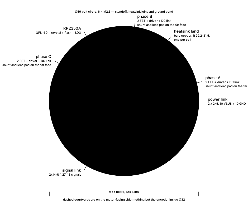
tools/geometry.py reads the same coordinates gen_boards.py writes
into the KiCad file. Solid courtyards are on the outward face, dashed ones on the
motor-facing face. The three phase cells sit at 60°/180°/300° so all three
commutation loops are the same shape; the three wedges between them carry the interconnect
and the CPU; the gold arcs at the perimeter are bare copper for the heatsink ring, and are
the reason every part stops at R 29.2. Nothing but the encoder and the motor screws
lives inside Ø32.| Item | Value | Where it comes from |
|---|---|---|
| Board diameter, both boards | Ø65.0 mm | Set 2026-09-07 |
| Motor mount | 4 × Ø3.2 (M3) at (±12.5, 0) and (0, ±9.5) | Inherited verbatim from hardware/encoder H1–H4 |
| Encoder centre | (0, 0) — coincides with the shaft axis | MT6701 sensing centre |
| Central keepout | R < 16 mm, both faces | Screw heads + magnet clearance |
| Sections | Three phase cells of 60° at 30/90/150°, adjacent, then three 60° wedges at 210/270/330° | Grouped rather than alternating, and narrowed — see below |
| Board-B mounting | 6 × M2.5 on a Ø59 bolt circle, on the six section boundaries: 0, 60, 120, 180, 240, 300° | Every section gets one at each edge — and at 60/60 that is an even circle again |
| Phase pads | 3 arcs, R 28.1–31.3 over 14°, 23 mm² each, at 30°/90°/150°, on B.Cu | 14 AWG motor leads. An arc, because a straight pad this wide at this radius puts its corners off the board |
| Heatsink land | 3 arcs, R 29.2–31.5 over 48°, plus six Ø4.8 mm bosses = 250 mm² of bare copper | §4 — the joint a heatsink would clamp, 0.33 K/W; kept although no fins are planned |
| Parts placed, board A | 124 by the floorplan — 69 outward, 55 motor-facing, 10 DNP — and 12 generated (lands, lead pads, bosses) | tools/placement.py |
| Netlist, board A | 136 components, 87 nets, 425 connections | tools/schematic.py, checked against the placement both ways |
| Usable annulus | R 16 → 31.5 = 2313 mm² per side | Computed |
| Board A stackup | 6 layer, 2 oz outer / 1 oz inner, 1.6 mm, 0.1 mm F.Cu→In1 prepreg | Same as the sister board, except the prepreg, which is what §1's 0.39 nH rests on |
| Board B stackup | 4 layer, 2 oz outer, 1.6 mm | No dense routing; 4 is enough |
| Standoff, motor face → board A | 10.75 mm | Derived: 5.0 shaft + 2.5 magnet + 1.5 air gap + 1.75 MT6701 body |
| Standoff, board A → board B | 11.0 mm | Board A parts + mated interconnect height |
| Total above the motor rear face | 36.0 mm | Connectors and bulk cans included |
- The CPU moves to the middle of the wedge group, as far from every switching node as a round board allows.
- The three motor leads leave together, so one bundle leaves the enclosure through one hole instead of three.
- The DC bus feeds one contiguous 210° block from the power link at its edge, rather than reaching around the board past the CPU.
The six M2.5 sit on the six section boundaries, so every section has a bolt at each edge and every phase cell's heatsink land runs the full width between its own two. At 70/50 that cost the even spacing; at 60/60 it does not, and the bolt circle is regular again.
The six boss pads sit on R 26.9–32.2, and between them that band is empty: the heatsink land owns it on the outward face, and on the motor-facing face nothing but the lead pads wants it. So everything without a reason to be somewhere in particular now lives there at R 29.3 — the bootstrap diode (only its capacitor has to be at VB and VS), the DC-link 100 n, both input pulls, and each phase's clamp diode, which ends up beside its own lead pad. The DC-link bulk ceramic moved to its own row at R 26.8, as far out as the land allows.
That held for the utility wedges and not for the phase cells. Routing found that a part in a phase cell's channel can be connected only if its nets are GND or the phase output — the phase-output pour owns B.Cu beneath it, the heatsink land owns F.Cu above it, and the bosses cut the outer ring into six arcs. Five of the six went back into the cell and the cells were widened to 68° to take them. The clamp diode stayed, because its nets are exactly the two that work. §10b has the measurement.
| 70° cells | all in the channel | now | |
|---|---|---|---|
| Phase cell | 70° | 60° | 68° |
| Utility wedge | 50° | 60° | 52° |
| Phase group | 210° | 180° | 204° |
| Bolt spacing | 70/70/70/50/50/50° | 60°, even | 68/68/68/52/52/52° |
| In the channel, per cell | — | 6 parts | 1, the clamp diode |
| Heatsink land | 286 mm² | 250 mm² | 279 mm² |
Three consolidations paid for it: the per-driver 1 µF VCC bulk became one 4.7 µF at the power link (three of them on one 0.1 A rail was two too many), the lead pad narrowed from ±8.5° to ±7° — 23 mm², still ample for a 14 AWG lead — and the row packer learned to dodge parts in other rows, because two rows that overlap radially and sit at different angles can collide and a packer that only looks at its own row walks straight into them.
Area is not the constraint. The sister board fits a four-bridge stage, a twelve-pin switched encoder port, isolated CAN and USB-PD into roughly 4400 mm² of courtyard across two sides. This design has four usable sides of 2313 mm² and far less to put on them. That buys the right to keep thermally generous packages instead of chasing the shrinks in the sister project's F-47 — take the small parts where they are also better parts, not merely smaller ones.
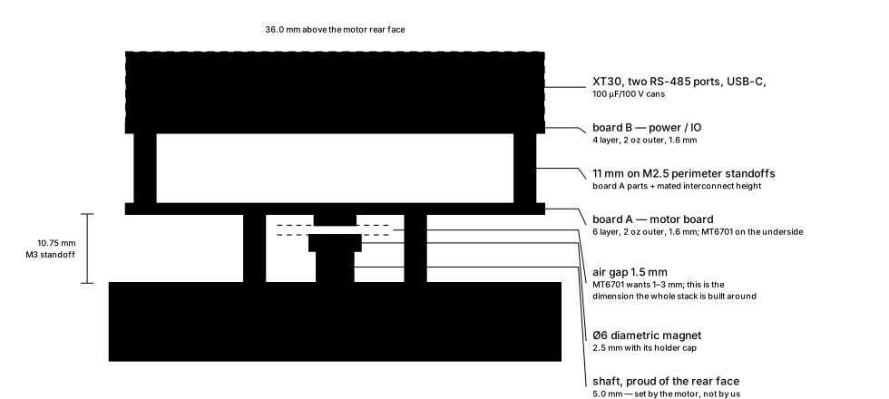
tools/geometry.py once the motor is known and every dimension here follows.3 · Power stage
| Bus voltage | 60 V nominal, 12 V minimum (decided 2026-09-22), 80 V silicon throughout, TVS breakdown 71–79 V |
|---|---|
| Phase current | 20 A RMS per phase — the figure everything is sized to, and since 2026-09-22 a burst figure rather than a continuous rating (§4) — 28.3 A peak, ±32 A of sense. Draft 0.2 used “20 A” for the RMS figure in §4 and for an instantaneous one in §5; they differ by √2 and the sense chain lost. One number now. |
| Switching frequency | 20 kHz nominal (the number every estimate below is quoted at) |
| Topology | Three independent half-bridges, software dead time, inline phase-current sense |
| Function | Part | Rationale |
|---|---|---|
| MOSFET, 6 × | BSC030N08NS5, PowerPAK SO-8 | Unchanged. 80 V, 2.6/3.4 mΩ at VGS = 10 V, 100% avalanche tested, 27k in stock at LCSC. Driven properly this time — see the row below. |
| Gate driver, 3 × | EG2103, SOP-8 | Changed. The sister board's EG3113 is unbuyable — 9 in stock, minimum purchase 25 (their F-40, which blocks its ordering). The obvious like-for-like replacement, EG2131, turns out to be also out of stock. EG2103 is the same EG Micro family and the same logic convention, 2,225 in stock, MOQ 5, $0.19 @100: 600 V, VCC 10–20 V, interlock plus 560 ns internal dead time, HIN active-high with a 200 k pull-down, LIN active-low with a 200 k pull-up. It needs the 12 V rail, and that is the point. What it gives up is drive strength — ±0.3/0.6 A against EG3113's 2/2.5 A — costed in §4. |
| Gate rail | 12 V, its own buck on board B | Changed. This is the single largest improvement available and it is quantified in the sister project's F-41: driving a 10 V-rated FET from a 5.04 V rail costs ~2 W per bridge of switching loss and ~15% on RDS(on). See §4. |
| Gate network | 2.2 Ω + 10 k G–S, PNP booster DNP | Changed, because the driver is now the limit rather than the resistor. EG2103 saturates at 0.3 A, and reaching that from a 12 V rail needs Rg ≈ 28 Ω — so below about 28 Ω the resistor buys no speed at all and only adds turn-off delay against the 0.6 A sink. 2.2 Ω is therefore for gate-loop damping, not for edge shaping. Footprints kept for the sister board's PNP turn-off booster (their Q1 + D6/D7), which is the proven way to buy the turn-off edge back if §4's switching term proves binding on the bench. |
| Current sense, 2 × | INA241A3, TSOT-23-8, 50 V/V | Changed. Higher gain lets the shunt shrink. Inline, not low side, so torque is measurable at standstill and at any duty cycle. The package is TSOT-23-8 (the DDF suffix), not the SOT-23-8 draft 0.2 wrote; that is what is placed on board A. A third footprint sits on phase C, DNP — there is no fourth ADC channel for it. And the grade is A3. INA240 numbers its gains A1 = 20, A2 = 50; INA241 numbers them A1 = 10, A2 = 20, A3 = 50. Draft 0.2 carried the INA240 mapping across and asked for a 20 V/V part to do a 50 V/V job — table 4-1 of the INA241A datasheet. |
| Shunts, 2 × | 1.0 mΩ (2 × 2 mΩ 2010) | Changed again, and this one is a correction rather than an improvement. Draft 0.2's 1.6 mΩ was chosen to reproduce the sister board's 80 mV/A so firmware constants would carry across. It gives ±20.6 A of full scale, and the design point peaks at 28.3 A: the chain would have clipped on every cycle above 14.6 A RMS. 1.0 mΩ × 50 V/V = 50 mV/A → ±29.0 A worst case, 2.5% over the peak, and costs 0.80 W instead of 1.28 W — the 0.8 mΩ pair this row carried until 2026-09-24 has no stocked 1.6 mΩ 2010 to build it from. Phase C gets the same two footprints as 0 Ω links so all three phases match. See §5. |
| Phase TVS, 3 × | TPSMF4L64A, SOD-123FL | Same 64 V standoff / 400 W as SMAJ64A (their F-09 fix) in a much smaller package — one of the F-47 swaps that is worth taking. |
| DC-link ceramic | 6 × 2.2 µF 100 V 1206 + 6 × 100 n | New requirement created by putting the bulk on board B. Two of each per cell, flanking the FET pair tangentially inside the commutation loop. §1 now has the measurement that justifies them: 0.39 nH of PCB loop, 1.7 V of overshoot. |
| Input pulls, 6 × | 4.7 k on every HIN and LIN | New, and not optional. Two errata meet on this pin. EG2103's LIN is active-low with an internal 200 k pull-up; RP2350's GPIOs leave reset as inputs with a ~60 k pull-down, and erratum E9 can latch a Bank 0 input near 2.1–2.2 V. The divider of those two lands LIN around 1.2 V — above VIL 1.0 and below VIH 2.5, which is the one place a gate driver input must never sit. 4.7 k to GND on both HIN and LIN makes the reset state a property of this board instead of two other people's errata, and ≤9 k is also the documented E9 workaround. To GND on both is the brake-on-reset decision of 2026-09-22 (the box below); until then LIN went to +3V3, for a coast. They sit on the driver's logic side, one via each. |
| RC snubber, 3 × | 2.2 Ω + 470 pF C0G 100 V, 0603, DNP | New, footprints only. The simulation's answer to the one corner that fails: if the EG2103's output stage is the strong one, the turn-on ring reaches 73.9 V of Vds; this across the switch node takes it to 62.7 V for 0.034 W per cell (sim P2, Q3). Fitted only if the driver measures strong. On the back under the high-side FET, the resistor's pad on the switch-node pour and the capacitor's on a ground via, their middle node a pour of its own. 0603 rather than the 0805 the simulation proposed, because an 0805 pair does not fit between the sense tap and the shunt; the ratings do not need 0805. |
Every changed row above is a sourcing risk until checked. The sister
project's F-40 is precisely the failure of not doing this: a design that cannot be ordered
because one part has nine in stock. Before any of these reach a schematic symbol, confirm
LCSC stock depth and minimum buy for INA241A2 — F-47 verified the A1 in
SOT-23-8, not the 50 V/V grade, which is INA241A2IDDFR in TSOT-23-8;
INA240A2PWR (C129949) is in stock as a fallback but is TSSOP-8 and only
±80 V common mode against INA241's ±110 V, so it is a different footprint and
less margin on a 60 V phase node —
2.0 mΩ 2010 shunts at 1% or better, TPSMF4L64A,
LMR38010, and the ripple-rated bulk §8 now needs. F-47 already notes
that ISO1044 "is absent from the JLC in-stock listing today" despite being the recommended
swap; assume nothing.
Checked 2026-09-07, and the results are why this box exists: EG2103 C480654 — 2,225, MOQ 5, $0.19, but only 0.3/0.6 A drive; FD2103S C5187182 — out of stock, and it was the cheapest hit; EG2131 C193777 — not available; UCC27282DR C2867844 — 1,227, $1.99; NCP5183DR2G C904511 — 2,883, MOQ 1, $0.92, but 4.3 A and no interlock. EG2103 chosen: the interlock and the 560 ns dead time are worth more here than the edge rate. Three of the five first-choice parts were unbuyable or overpriced. The 40 V-class question does not arise here, but no confirmed high-stock 80 V alternative to BSC030N08NS5 was sought — it has 27k in stock and stays.
- Its truth table is unambiguous: HIN = LIN = 0 turns the low side on, HIN = LIN = 1 turns the high side on, and any disagreement turns both off. LIN is active-low, as §6 assumed.
- Its block diagram draws 200 k from an internal +5 V into LIN, and 200 k from HIN to ground.
- Its parameter table agrees: Iin(L) is specified as −10 µA at Vin = 0 V. Current flowing out of an input held low is a pull-up, and it is a guaranteed number rather than a drawing. Quiescent current is also specified with the inputs floating, which is not how you characterise a part whose floating state turns a MOSFET on.
- Its prose, in §2, says LIN has a 200 k pull-down — and then finishes the same sentence by claiming floating inputs turn both MOSFETs off, which is only true if it is a pull-up. It is a copy-paste of the HIN clause. EG Micro's website has the corrected wording; LCSC's summary repeats the typo.
RUN low is a
real hardware stop. Three independent statements in the manufacturer's own document
against one self-refuting sentence.
That is the die. The board still needs the six 4.7 k pulls in the parts table, for a different reason: RP2350's reset-state pull-down fights EG2103's 200 k pull-up and parks LIN in the undefined band. The datasheet answer and the erratum answer are not the same answer.
Decided 2026-09-22: a reset brakes. Both pulls go to GND, and
HIN = LIN = 0 is the truth table's low-side-on state, so while the CPU is
in reset — RUN low, a watchdog, a brown-out, the first milliseconds of boot
— every low side conducts and the motor is shorted through its own windings. 4.7 k
against the 200 k internal pull-up holds LIN at 0.11 V. Two things follow that are easy to miss.
The brake lasts only as long as the 12 V gate rail: GATE_EN comes from a GPIO,
which is an input with a pull-down in reset, so board B has to hold the gate rail on by
default — a pull-up on the buck's EN that the CPU can pull down — or a
reset becomes a brief brake and then a coast. And a brake is not a stop on a joint that is
still being driven: it turns the load's energy into winding current, which is also why it
does not pump the bus the way a regenerating decel does (question 8).
4 · Thermal — what 20 A costs
Board A is a sealed sandwich: its inner face looks at the motor, its outer face looks at board B. Neither sees moving air. Everything else in this spec is comfortable; this is not, and committing to 20 A RMS continuous is a decision about the enclosure as much as about the board.
| Term | Sister board 5 V gate rail, 4 mΩ × 3 |
This spec 12 V gate rail, 1.0 mΩ × 2 |
|---|---|---|
| At 20 A RMS per phase — the design point | ||
| Conduction, 3 bridges | 6.6 W | 5.69 W |
| Switching, 3 bridges | 6.0 W | 3.84 W |
| Shunts | 4.8 W (3 phases) | 0.80 W (2 phases) |
| Gate charge + driver quiescent | 0.7 W | 0.14 W |
| RP2350A, LDO drop, MT6701, amplifiers | 0.26 W | |
| Total | 18.1 W | 10.72 W |
| At 10 A RMS per phase | ||
| Total | 6.6 W | 4.28 W |
The switching row is where the driver choice lands. EG2103 sources 0.3 A and sinks 0.6 A, so against a 19.5 nC Qgd the edges are 65 ns on and 32 ns off and no gate resistor below about 28 Ω changes that. Add the complementary body diode's 188 nC of reverse recovery at 60 V and the three bridges come to 3.84 W. A 4 A driver would save roughly 2 W across the board; that 2 W is the price of the hardware interlock and the 560 ns dead time, and it is a deliberate purchase.
The path out, in four resistances
| Step | K/W | ΔT | What sets it |
|---|---|---|---|
| Junction → drain pad | 0.9 | 1.4 K | RthJC max, PG-TDSON-8 |
| Drain pad → inner copper | 7.6 | 12.1 K | 16 vias of 0.4 mm in the drain pad, 0.95 mm pitch — the low side; the high side has 20. The FR4 alone would be 354 K/W |
| Phase cells → perimeter bosses | 1.0 | 10.7 K | Spreading in six layers of copper |
| Bare copper → heatsink | 0.4 | 4.3 K | 286 mm² of mask-free land through a 0.25 mm gap pad |
| Heatsink → ambient | ≤ 6.67 | ≤ 72 K | Everything left over, for Tj ≤ 125 °C at 25 °C ambient |
So §4 of draft 0.2 asked which of four options to take, and the answer is option 2, taken seriously. The machined aluminium ring is not an optional upgrade that buys headroom — it is a structural member of the thermal design, and the board is now laid out around it:
- Every part on the outward face stops at R 29.2, leaving an uninterrupted annulus for the ring to clamp.
- Each phase cell offers a 58° arc of mask-free copper at R 29.2–31.5, between that cell's two perimeter bolts. With the six Ø4.8 mm bosses that is 286 mm² of metal-to-metal joint.
- The six M2.5 holes are plated, with pads on every layer and mask open both sides. They are the standoff, the heat path and the chassis ground bond at once.
- The motor leads land on the motor-facing face, so the ring needs no notches and the outward perimeter is entirely thermal.
Options 3 and 4 from draft 0.2 stay declined for the reasons given there: the motor housing is the hotter body in the case this drive exists for, and a finned lid on board B is on the wrong side of an 11 mm air gap. The ring is the only path that leaves board A's copper through metal.
5 · Sensing
The RP2350A has four ADC inputs, on GPIO26–29. That is the whole analog budget, and it is spent as follows.
| Channel | Signal | Chain |
|---|---|---|
| ADC0 / GPIO26 | Phase A current | 1.0 mΩ inline → INA241A3 ×50, 1.65 V referenced → ±29.0 A |
| ADC1 / GPIO27 | Phase B current | as above |
| ADC2 / GPIO28 | Bus voltage | 50 k / 5.1 k 0.1% divider on board A, where VBUS already is |
| ADC3 / GPIO29 | FET temperature | 10 k NTC in the phase-cell copper pour |
| ADC4 (internal) | Die temperature | free, and a usable ambient proxy |
Phase C current is reconstructed as Ic = -(Ia + Ib). What that costs is worth
stating plainly: no per-phase fault detection, no redundancy, and any offset error in A and B
lands doubled on C. For FOC on a wye-connected motor it is standard and sufficient.
A second NTC footprint sits by the motor mount pattern, DNP, with a 0 Ω jumper selecting which thermistor reaches ADC3 — so motor-housing temperature is a build option rather than a respin.
It took two goes. The first correction was 1.0 mΩ for ±32 A, sized against the amplifier's typical output swing. The datasheet's worst case is VS − 0.2 V rather than 0.07 V, and that turns ±32 A into ±29 A — 2.5% over a 28.3 A peak, which is not margin.
Then: 0.8 mΩ (2 × 1.6 mΩ 2010) × 50 V/V = 40 mV/A → ±36.2 A worst case, 28% clear of the peak, and a precision mode (one of each pair desoldered) at exactly the sister board's 80 mV/A.
Now, since 2026-09-24: 1.0 mΩ (2 × 2 mΩ 2010) × 50 V/V = 50 mV/A → ±29.0 A worst case, at 0.80 W. Sourcing found no 1.6 mΩ 2010 at LCSC or JLCPCB — 1 and 2 mΩ, nothing between — so the chain is back at the 2.5% the first correction was turned down for, taken knowingly; the stocked alternative, 2 × 1 mΩ, reads ±58 A at 25 mV/A. The precision mode is now 2 mΩ, 100 mV/A, ±14.5 A, and neither mode is the sister board's scaling. Keep the table in the README and the firmware define pointed at each other; F-14 is what happens otherwise.
tools/placement.py checks all of it, including the cross-layer case a
same-side courtyard check cannot see.
6 · Control — RP2350A
Thirty GPIO, of which this design uses twenty-one. QSPI flash, USB, SWD and the crystal all sit on dedicated pins and cost nothing from that budget.
| GPIO | Net | Note |
|---|---|---|
| 0, 1 | RS485_DI, RS485_RO | UART0 TX/RX, via the interconnect to board B |
| 2 | RS485_DE | Transmit driver enable; firmware- or PIO-timed |
| 3 | RS485_TERM_EN | Optional switched termination — see §7 |
| 4, 5, 6 | ENC_SCK, ENC_CS, ENC_DO | SPI0 to the MT6701 in SSI mode. No MOSI: the sensor only talks. |
| 7 | ENC_OUT | MT6701 OUT pin — ABZ or PWM alternate, spare otherwise |
| 8, 9 | HIN_A, LIN_A | PWM slice 4, channels A and B |
| 10, 11 | HIN_B, LIN_B | PWM slice 5 |
| 12, 13 | HIN_C, LIN_C | PWM slice 6 |
| 14 | GATE_EN | The 12 V rail on board B. Defaults on through a reset, so that a reset brakes (§3); firmware pulls it low to kill the gate drive |
| 15 | FAULT_n | Overcurrent comparator, in — populate/DNP option |
| 16, 17, 18 | LED_R, LED_G, LED_B | Plain RGB LED on board B |
| 19 | PD_INT_n | FUSB302 interrupt |
| 20, 21 | PD_SDA, PD_SCL | I2C0 to the FUSB302 on board B. This was SDA on 19 and SCL on 20, which are I2C1's SCL and I2C0's SDA — not a hardware I²C pair. Fixed 2026-09-22 by rotating the three names on the routed copper; J9 pins 9, 10, 12 are now INT, SDA, SCL. 20–23 are also SPI0 RX, CSn, SCK, TX |
| 22 | USB_VBUS_DET | Was spare. Board B sends it, and nothing on board A was listening |
| 23–25 | spare | Three free, on test points TP1–TP3 |
| 26–29 | ADC0–3 | §5 |
Two details in that table are doing real work.
Each half-bridge sits on one PWM slice, and both its inputs carry the same
waveform. GPIO 8/9, 10/11 and 12/13 are the A and B channels of slices 4, 5 and 6.
Because EG2103's LIN is active-low, the driver does the inversion internally: its truth
table has HIN = LIN = 0 turning the low side on and
HIN = LIN = 1 turning the high side on. So PWM_CH_CSR.B_INV
stays clear and both channels run the same duty. Dead time comes from the
driver's own 560 ns, not from offsetting the compare values — and §3 now has the
datasheet's truth table confirming that reading. Two consequences for the loop: the driver adds
780 ns of turn-on delay against 220 ns of turn-off, which is the dead time rather than
a circuit alongside it; and an input pulse shorter than about 560 ns produces no output, so at
20 kHz the bottom and top 1.1% of the duty range are unreachable.
Get the polarity backwards and nothing dramatic happens, which is the nice consequence of an
active-low LIN: B_INV set would drive HIN and LIN oppositely, which the truth
table resolves as both-off or a fight the interlock wins — not a shoot-through. Still bring up
on a current-limited supply with no motor attached.
The status LED is three GPIO, not a WS2812. The sister project's F-16 is a WS2812B needing VIH = 3.5 V from a 3.3 V GPIO, fixed by dropping the LED supply through a Schottky. With spare GPIO and no 5 V rail on board A, a plain RGB LED is smaller, cheaper and has no failure mode.
7 · Board B — power and I/O
Power tree
SOURCES ──────────────────────────────────────────────────────────────────

  XT30, 12–60 V ──────────────────────────────────────────→ VMOT
                  straight through, so regen can reach the pack

  USB-C VBUS ─┬─ FUSB302BMPX ── I²C ── CPU      PD sink, ≤ 20 V / 5 A
              │
              ├─ LTC4359 + E100N4P0HL1 ────────────────────→ VMOT
              │     ideal diode; blocks VMOT from the USB host.
              │     PD powers the drive instead of a pack, not with one
              │
              └─ Schottky ──────────────────────────────→ 5 V Vlogic
                    pre-contract path: logic only, no gate rail


RAILS ────────────────────────────────────────────────────────────────────

  VMOT ─┬─ SMDJ64A TVS  +  3 × 100 µF / 100 V bulk
        │
        ├─ the three half-bridges, board A
        │
        ├─ LMR38010 ──→ 12 V  Vgate   0.1 A    EG2103 × 3, board A
        │     EN pulled up: on unless GATE_EN pulls it down
        │
        └─ LMR38010 ──→  5 V  Vlogic  0.5 A ──→ SPX3819 ──→ 3.3 V
                                                  RP2350A + MT6701, board A
Two independent bucks off VMOT rather than a cascade. Same part twice, and a fault in the
gate rail does not take the CPU down with it. Both are LMR38010 (4.2–80 V, 1 A
synchronous), F-47's recommended replacement for the sister board's XL7005A. The 12 V rail is
enabled by GATE_EN from the CPU — on by default, with a pull-up
the CPU can override, because a reset is meant to brake and a brake needs the gate rail
(§3). Both regulate happily from a 20 V VMOT as well as a 60 V one, which is what makes
the next section work.
VMOT runs down to 12 V (decided 2026-09-22), and that is the one place the gate rail does not regulate: the LMR38010's maximum duty cycle is 97%, so at a 12 V bus the 12 V rail sits in dropout near 11.5 V. That is still above EG2103's 9.7 V VCC turn-on, the bootstrap reaches about 10.6 V against the 9.6 V VB turn-on, and the FETs see about 11 V of gate against the 10 V their RDS(on) is specified at. Below 12 V none of that holds, which is why 12 V is the floor rather than a nominal.
| Source | VMOT | 12 V gate rail | What the drive can do |
|---|---|---|---|
| USB, no contract yet | 5 V | down | Logic, encoder, RS-485 up. Motor cannot energise. Configuration and bring-up. |
| USB-PD, 20 V contract | 20 V | up | Full control at reduced voltage, capped by PD at 100 W (20 V × 5 A, e-marked cable). |
| USB-PD, 12 or 15 V contract | 12–15 V | up (dropout at 12) | As above, at lower power. Useful now that VMOT's floor is 12 V. |
| XT30 battery | 12–60 V | up | Full performance at 60 V. |
The pre-contract state is not an accident to preserve — it is the direct consequence of a buck that cannot make 12 V from 5 V, and it means bench work on a board with no battery attached is physically incapable of spinning the motor until firmware asks for the voltage.
Full-duplex RS-485, two ports
Four-wire RS-485, so the master can transmit whenever it likes and only the drives need to arbitrate. Two connectors wired pin-for-pin in parallel: the cable runs in one and out the other, and the bus is a bus, not a repeater chain. No firmware is in the path of a pass-through, so an unpowered or crashed drive does not break the run below it.
| Pin | Net | Direction, from the drive's point of view |
|---|---|---|
| 1 | GND | — |
| 2, 3 | DOWN+, DOWN− | master transmits, every drive receives |
| 4, 5 | UP+, UP− | one drive transmits at a time, master receives |
| 6 | GND | — |
Naming the pairs by direction rather than by A/B is deliberate: a straight cable then wires itself correctly, and there is no crossover to get wrong at 3 a.m.
Two SIT3088ETK (DFN-8, already sourced by the sister project) rather than one
full-duplex part: one strapped permanently as a receiver on the DOWN pair, one as a driver with
DE on the UP pair. Cheaper than a MAX3491, in a package that is already in the
library, and it puts the failure modes somewhere already understood.
- Termination is per-node, not per-board (their F-19). 120 Ω across each pair behind a solder jumper, open by default. Only the two ends of the chain bridge them. A board that terminates unconditionally breaks every mid-bus installation.
- Fail-safe bias must be computed against the termination, not guessed (their F-01). Their 10 k/10 k idle bias delivered ±32 mV differential into a 100 Ω termination against a −200…−100 mV receiver threshold. Size the bias for >200 mV differential with the termination present, or use the SIT3088's own fail-safe and prove it on the datasheet.
USB-C
Full USB-PD sink, as on the sister board: FUSB302BMPX negotiating over I²C from
the CPU, up to a 20 V / 5 A contract. The sister project's two highest-severity power findings
are both PD front-end bugs, and both have adopted fixes that come across as fixes rather than as
problems to rediscover:
- F-27 — the backfeed blocker. Their LM74700 is a 65 V part with its cathode
sitting on a 60 V VMOT: five volts of margin against a rail that regen actively pumps upward,
and a failure mode that connects the motor bus to a laptop. Adopted fix, taken here verbatim:
LTC4359CMS8(4–80 V operating, 100 V abs-max pins) driving anE100N4P0HL1(100 V, 4 mΩ, PDFN5×6), which also keeps the 5 A path under 0.1 W where a Schottky would burn 2.75 W. - F-39 — the ESD part. USBLC6-2P6 references its steering diodes to pin 5, which has an internal ~6 V zener; on VBUS that survives 5 V and dies the first time a 20 V contract is agreed. Pin 5 goes to +3V3, and VBUS gets its own clamp at the connector, sized against FUSB302's ~28 V VBUS absolute maximum.
The 20 V capability is the reason to be careful here rather than a reason to drop PD: it is also what makes the drive useful on a desk with nothing but a laptop charger.
8 · Interconnect
Two connectors, so the 60 V bus never runs beside USB or SWD. The signal count is set mostly by keeping PD on board B: the FUSB302 sits next to the USB-C connector where the CC lines are short, but the CPU that negotiates with it is on board A, so its I²C and interrupt cross the interconnect.
| Connector | Carries | Rating |
|---|---|---|
| Power link — 2 × (2×5) @ 2.54 mm, stacked radially | 10 × VBUS, 10 × GND, ganged | 30 A at 3 A/pin, against 23.2 A RMS — see below |
| Signal link — 2×14 @ 1.27 mm | +12 V, +5 V, USB D+/D−, USB_VBUS_DET, PD_SDA, PD_SCL, PD_INT_n, RS485 DI/RO/DE, RS485_TERM_EN, SWCLK, SWDIO, RUN, BOOTSEL, LED × 3, GATE_EN — 20 signals, 8 interleaved grounds. Draft 0.3 said 18 and 10; nobody had counted. USB sits at position 3 with a ground either side. | signal |
Two 2×5 headers stacked radially fit the same 50° wedge, mate together, and give
30 A. geometry.interconnect() is the calculation, so changing the design point
moves it.
The six perimeter screws do the alignment and carry the mechanical load; the connectors only have to mate. Their mated height and the standoff length are the same dimension and must be ordered as one decision. Note that the screws are now plated and grounded on both boards for §4's sake, which puts six brass standoffs in parallel with the header's ten ground pins — free return path, and a reason the link is less stressed than the arithmetic above assumes.
An alternative worth pricing before committing: make two of the six perimeter standoffs the power path — brass, into generous plated pads on both boards — and drop the header entirely. It is mechanically cleaner and electrically excellent if the joint is sound, and the whole question is whether a screwed joint's contact resistance is trustworthy over thermal cycling. Not the kind of thing to adopt without a bench test — and it now collides with §4, which wants all six of those screws carrying heat and ground, not two of them carrying 60 V.
9 · What this inherits, and what it fixes
The sister project's findings register is the most valuable thing it hands over. These are the rows that apply to a board that has not been built yet.
| Their ID | What it says | What this board does |
|---|---|---|
| F-40 | EG3113 unbuyable — 9 in stock, min purchase 25; blocks ordering | Designed out — on the third attempt. EG2131 was the obvious swap and is also out of stock; EG2103 (C480654, 2,225, $0.19) keeps the family, the logic convention, the interlock and the dead time. |
| F-41 | 10 V-rated FETs driven at 5.04 V: ~2 W/bridge switching, ~15% on RDS(on) | Designed out. 12 V gate rail, which EG2103 requires anyway (VCC 10–20 V). Halves the sister board's 95 ns edges to ~50 ns; the rest of the gap needs a stronger driver, not a higher rail. |
| F-16 | WS2812B VIH 3.5 V vs 3.3 V GPIO | Designed out. Plain RGB LED on three GPIO. |
| F-27, F-39 | USB-PD front end: 65 V blocker on an 80 V bus; USBLC6 pin 5 on a 20 V rail | Inherited as fixes, not as bugs. PD stays — 20 V feeds VMOT. LTC4359 + E100N4P0HL1 per their adopted F-27 disposition; USBLC6 pin 5 to +3V3 per F-39. |
| F-17 | E-stop is a bare GPIO; a wedged CPU cannot be stopped | Structural. EG2103 floats to both-FETs-off, so RUN low is a real
stop. But their disposition says it brakes, and per the EG3113 datasheet it coasts
— see below. |
| F-14 | Shunt value drifted out of sync between schematic, board, firmware and README | Process, not silicon. One table, in the README, referenced from the firmware define. |
| F-19 | No on-board bus termination; isolation only worked if the harness cooperated | Applied to RS-485: jumpered 120 Ω, open by default. |
| F-01, F-02, F-03 | Encoder-port bias, termination and floating-mux failures | Mostly moot — no encoder port. The bias/termination arithmetic carries to RS-485. |
| F-06 | MT6701 SSI response shifted by transceiver round-trip delay; ~2–4 MHz ceiling | Moot. The sensor is on the same board as the CPU; no line drivers, no round trip. |
| F-47 | Space-budget study: same-function package swaps and architectural shrinks | Cherry-picked. TPSMF4L64A, INA241, LMR38010, 2010 shunts — taken. LMG1205 — declined, it locks the gate rail at 5 V, which is the thing F-41 says to stop doing. |
| F-40, again | The lesson generalises: three of five first-choice parts here were unbuyable or overpriced when actually checked | Every non-inherited part carries its LCSC number and a dated stock figure in §3. Re-check before ordering; these numbers rot. |
| F-48 | JLCPCB process: free POFV on 6-layer, 0.10 mm rules, via spacing trade-offs | Decide before the first placement run, not after. |
Three things are worth handing back. The first is a correction to draft 0.2 of this document rather than to their register.
Their board carries R1, R2, R21 and R22:
four 10 k pull-downs, on both inputs of two EG3113s, straight to GND
(A_PWM_H/A_PWM_L on U1, B_PWM_H/B_PWM_L on
U6, pins 2 and 3 in both cases). EG3113's LIN is active-low with an internal 200 k pull-up.
10 k beats 200 k twenty to one, so LIN is held low, which is active, which
turns the low-side FET on. Their E-stop brakes, exactly as F-17
says — because of four resistors, not because of the driver.
What is worth handing back is what their register does not say: this is not only the E-stop behaviour, it is the power-up behaviour. Their bridge shorts the motor through its low-side FETs from the moment the gate rail is alive until firmware takes the pins, with no current limit and nothing sequencing it. On a spinning motor that is a braking current set by winding resistance alone. If that is wanted it should be written down as a choice; if it is not, it is four resistors.
This board went the other way at first — 4.7 k up on LIN, so reset coasted — and since 2026-09-22 it brakes like theirs, but as a written-down choice: both pulls to GND, and the gate rail held on through a reset so the brake is real (§3). On power-up the gate rail comes up with the CPU still in reset, so this board too shorts the windings through the low sides until firmware takes the pins. On a motor at rest that is nothing, and it charges the bootstrap capacitors on the way.
RP2350 erratum E9 reaches the gate driver, and that is the second. A Bank 0 GPIO can latch around 2.1–2.2 V, and at reset the pin is an input with a pull-down; against EG Micro's internal 200 k pull-up on LIN the divider lands near 1.2 V, between VIL and VIH. Their four pull-downs happen to defeat both at once. Anyone copying the circuit without them — as draft 0.2 of this spec proposed to — puts a gate driver input in the undefined band. The answer is an external pull in whichever direction you want, sized ≤ 9 k, and stated in the schematic.
F-40 needs a replacement driver regardless. EG2103 is the cheap like-for-like, but for their four-bridge board NCP5183DR2G is probably the better answer: 600 V, 4.3 A both ways against EG3113's 2/2.5 A, matched 120 ns propagation delays where EG3113's are asymmetric — their own F-41 notes its working margin comes mostly from that asymmetry — plus 50 V/ns dV/dt immunity, AEC-Q100, $0.92, MOQ 1, 2,883 in stock. It gives up the interlock and the internal dead time, which their GaN evaluation already argues they do not lean on. This board took EG2103 instead precisely because it is not thermally tighter than they are and can afford to keep the interlock.
F-41's remedy, a 12 V rail, is the last — harder there than here, because thirteen TS5A3159 analog switches sit on their 5 V rail at 5.5 V max. Worth noting it only buys about half the gap on its own: with EG3113's 2/2.5 A the resistor still sets the edge, so the rail and the resistor sweep in F-41 are complementary, not alternatives.
10 · Layout and capture — board A
Board A is placed, captured and routed: 136 parts, 87 nets, 425 pin connections, 78 on the outward face and 58 on the motor-facing face, ten DNP. Every connection is made; DRC finds nothing, ERC finds nothing, and KiCad's own exported netlist matches the one this repo intended — net by net, connection by connection. §10b is the routing.
The schematic is generated from a netlist in Python, not drawn: a component
is a reference, a symbol, a value, a footprint and a pin-to-net map, and
tools/schematic.py emits four hierarchical sheets from that. The sheets are drawn
with labels rather than wires — every pin gets a 2.54 mm stub and its
net's name. That is an honest description of what it is: routing wires between 115 parts
automatically produces something worse to read than a table. What it buys is that the
designators, the footprints and the DNP flags are one source of truth, checked in both
directions on every build. gen_boards.py will not write a board if a part is on it
and not in the netlist, or in the netlist and not on it, or if their footprints disagree, or if
any symbol pin has no net.
- The RP2350A was missing everything it cannot run without. No inductor
on
VREG_LXfor the core buck, no cap on DVDD, no filter onADC_AVDD, no pull-up or cap onRUN, no series resistor onXOUT. Eight parts — and the decoupling moved to the back, directly under the power pins, where the loop is the board thickness rather than a trip around the QFN. - The bus divider was wrong by 2.3×. 50 k / 5.1 k puts 5.5 V on a 3.3 V ADC pin at a 60 V bus. It is 112 k / 4.7 k now — 2.42 V at 60 V, 3.18 V at the TVS clamp — and the high leg is two resistors, because a 0603 is rated 50 V working and the bus is 60.
FAULT_nfloated. The overcurrent comparator is §11's open question, and not fitting it left a CPU input with nothing on it. A 10 k pull-up is the "not fitted" state.USB_VBUS_DETarrived from board B and went nowhere. It is on GPIO22 now.- The signal link is 20 signals and 8 grounds, not 18 and 10.
- The phase TVS were in §3's parts table and not on the board.
- The MOSFET's symbol and its footprint disagreed. KiCad's own
Transistor_FET:BSC030N08NS5numbers its pads 1–3 source, 4 gate, 5 drain; the sister project'sPowerPAK_SO-8_123numbers them 1/2/3 = S/G/D. Using both would have wired every FET wrong. Board A now takes KiCad's matched pair, which also has a larger drain pad and so an easier via array.
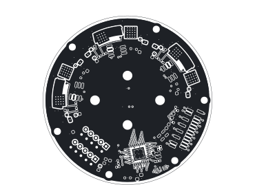
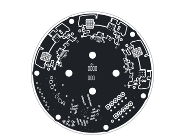
The phase cell
All three are identical, at 60°/180°/300°, so all three commutation loops are the same shape. Radially outward from the centre keepout:
| Band | R, mm | What is in it |
|---|---|---|
| Gate drive | 17.2–22.6 | EG2103 on the cell axis, turned so it costs the band 5.4 mm of radius instead of 7.4. The SOIC-8 pinout then sorts itself: VCC and the logic inputs land on one side, LO/VS/HO/VB on the other, so the supply parts get one side and the bootstrap the other. |
| Half-bridge | 23.1–28.6 | Both FETs at the same rotation, 3.75 mm either side of the axis, so the high side's source pads and the low side's drain pad end up adjacent: the switch node is a small island between them and VBUS and GND come out at the two far ends, where the DC link sits. Both are turned so the gate pad, at one end of the source row, sits at R 24.4 facing the driver row across an empty 1.5 mm, rather than at R 27.9 walled in by the switch-node pour and the heatsink land. Nothing else is in this row. |
| DC-link bulk | 24.5–29.1 | Two 2.2 µF 1206 flanking the pair, as far out as the heatsink land allows — same job, fewer degrees. (A 1210 ran into the perimeter boss once the cell was rebuilt for the fan-out.) |
| Heatsink land | 29.2–31.5 | Nothing. That is the point — see §4. |
- The low side's barrels all reach B.Cu now. The switch-node pour on the
back stopped at R 25.2, so only the inner row of the sixteen under each low-side drain
touched it; the other twelve sat in the clearance between it and the phase-output pour.
The pour now carries a tab over the whole array (
gen_boards.via_tab). - The high side has twenty barrels. A fifth row at 0.905 mm, the array moved 0.15 mm off the source side of the pad, and the via pad trimmed to 0.78 mm so it fits. Only the high side can take one: a fifth row under the low side comes 0.14 mm from the motor lead pad, and a fifth column under either comes into the shunts' courtyards.
- Snubber footprints, DNP, under the high side (§3's parts table).
- A Ø6 magnet rather than Ø8, as the MT6701 datasheet recommends; Ø8 over-drives the die at the short end of the gap. No board geometry reads the magnet's diameter, so this moved nothing but the drawings.
On the motor-facing face: the amplifier at the cell's centre with its SNSP tap and its filter cap clockwise of it within 0.4 mm of R 18.4, arranged for two arcs rather than for a router; the gate bleeds directly beneath the gate resistors, one via through both pads; the two shunts side by side under the switch-node island between the FETs' via clusters, their SW pads over the switch-node pour and their PHASE pads in the phase-output pour, because nowhere else on the back is clear of the DC-link caps' vias coming through; the arc lead pad at R 28.5–31.3; and the channel at R 29.3, holding the clamp diode.
Device:D numbers 1 = cathode, and the cathode was on +12V),
VREG_AVDD was tied straight to +3V3 where the reference filters it, and
USB had no series resistors. The crystal's load caps stay at 27 p where the
reference uses 15 p; the value is the crystal's to decide, and it is a different crystal.
How it is kept legal
tools/placement.py holds the floorplan and the rules it has to obey, and
gen_boards.py refuses to write a board if any of them fail. Parts pack into rows at
a radius; a row proposes a position and then walks it outward until the courtyards genuinely
clear, because two rectangles 0.3 mm apart along an arc are also rotated relative to each other
and can still have corners inside one another. On top of that it checks: nothing past
R 31.5 or inside R 16, nothing outside its own 60° sector, nothing touching a
perimeter boss pad, nothing on either arc, and — the one a same-side courtyard check cannot
see — no through-hole pad landing on a part on the other face. That last
rule is what found the FET thermal vias sitting on the shunts.
- Every pad needs its own absolute angle. KiCad does not derive pad orientation from the parent footprint. Leave it out and pad positions rotate while pad shapes do not — on a round board that is every fine-pitch part's copper turned the wrong way. It surfaced as a 1.27 mm-pitch SOIC-8 reporting 0.0000 mm between adjacent pins at 90° and nothing at all at 45°, and it would have been fabricated.
- A custom pad needs the angle separately, or its primitive polygon is evaluated unrotated — which put the heatsink lands off the board edge.
- Net classes want
microvia_*, notuvia_*, and apriorityon every class. Get it wrong and KiCad discards the list and silently uses its factory 0.2 mm netclass. The symptom is DRC quoting a clearance rule that appears nowhere in the project file. This one predates the layout work. - The stackup did not add up to 1.6 mm, also pre-existing. It does now, and the F.Cu→In1 prepreg is pinned at 0.1 mm because §1's loop inductance is quoted against it.
- A schematic's
lib_symbolsnames units by the bare symbol name. The entry isDevice:R, but its units areR_0_1, notDevice:R_0_1. Get it wrong and the sheet fails to load — and in a hierarchy that failure is silent: the root still opens, ERC still reports zero violations, and the netlist comes out empty. Nothing but exporting the netlist and counting would have caught it. - A sheet has two different uuids. The one inside the
.kicad_schis the file's; the path a symbol instance quotes is/plus the uuid of the(sheet ...)element in the root, with no root uuid in front. And the root's own sheet entries take(path "/"). - Two label stubs on one coordinate weld two nets together, quietly. The first layout pass put +12V and VB_A on the same point. Cells are sized from each symbol's own pin extent now, and the emitter refuses to place a label where a different net already sits.
One check is muted, lib_footprint_mismatch, and only that one: every footprint
is embedded verbatim from its library, but KiCad re-derives geometry through the placement
angle, so a part at 37.5° mismatches an identical library copy. Verified in isolation
before muting.
Three footprints are generated rather than drawn, from the same constants as everything else:
the PowerPAK SO-8 with its sixteen-via drain array, the M2.5 thermal boss, and the two arc pads.
Change FET_VIA_PITCH or the land radii in geometry.py and the
footprints follow.
10b · Routing — board A
Most of this board is not routed and was never going to be. Ground is two solid inner planes; VBUS is a sector of a third and +3V3 is the rest of that layer — the CPU wedge and the whole centre disc; each switch node and phase output is a pour on F.Cu and B.Cu, because 20 A does not go down a track and §4's IPC-2152 figure is about 6 mm of 2 oz copper. What is left is the signals, and those go to freerouting — less the ones it turned out to do badly, which are made first, as copper, and taken away from it.
Where it got to: 1361 track segments, 278 vias, and every one of the 425 pin connections made. DRC finds nothing, ERC finds nothing, KiCad's own exported netlist matches the intended one net for net. 212 of the vias are the tools' — 112 stitched into pads, the rest the fan-out's — and freerouting made the other 66. No foreign copper under the heatsink land, every annular ring legal, no right-angle corners. That is the 2026-09-22 board; the one before it was 1351 segments and 283 vias, and this one routed in freerouting's first round as that one did.
| 60°, in the channel | 68°, first pass | 68°, 2026-09-11 | 68°, this board | |
|---|---|---|---|---|
| Connections beyond a via in the pad | 170 | 170 | 146 | 143 |
| Left open | 74 | 101 | 0 | 0 |
| DRC | clean | clean | clean | clean |
| Right-angle corners | 2 | 0 | 0 | 0 |
The capacity was the lanes out of the QFN's via field, and it was countable. The escape vias sat in four rows 0.71 mm apart, and a 0.15 mm track passing radially between two rows needs 0.23 mm to clear a via's pad, 0.15 mm of clearance and half its own width on each side: 0.91 mm between row centres, and there was 0.71. No radial lane existed anywhere in the field, so all sixty escaped signals left through the tangential gaps within a row — 1.14 mm between two vias, which holds two tracks — and the last connections were the ones that ran out of them.
Two lines of the fan-out closed it. The outermost row moved out 0.20 mm, making that one gap 0.91 and buying a radial lane the whole way round the chip for 0.2 mm of depth. (A lane between every pair of rows wants 0.95 mm pitch, 3.5 mm of fan-out against today's 2.8, and another 0.6 mm of clear band on every side — the wedge rebuild again, one notch further. It was not needed.) And the pins the planned rows could not place get a second try from the generic escape, which does not mind which row a via lands in: one pin, LED_R, and a QFN pin without a via is a pin no router can ever leave, because the pads are 0.4 mm apart and a track with its clearance needs 0.45. With both, freerouting finished the board in its first round and the maze found nothing left to do.
The maze
The last few connections are not hard because the board is full. They are hard because they are last: the lanes out of the QFN's via field go to whichever nets reach them first, and what is left over cannot be routed by anything unwilling to move what is already there.
tools/finish.py rasterises the board — one bitmap per routable layer
(F.Cu, In3, B.Cu; In1 and In4 are ground and In2 the power planes) at 0.05 mm, every foreign
shape drawn and then grown by the clearance it wants, 0.15 mm or 0.4 for the 60 V nets, by a
distance transform. Then A* from one piece of the net to the other, eight-connected so every
step is 45°, with a via as a move between layers wherever a via fits; and the chain of cells
that comes back is folded into as few segments as the free space allows. The grid proposes and
the exact clearance test disposes: what it rejects is punched out and the route planned again.
Two things the maze must know that KiCad's clearance rules do not cover, both found
by DRC after the first run. The board edge — the clearance test is copper
against copper and the outline is neither, so the simplifier cut a corner 0.4 mm outside the
board. A bare drill — an M3 mounting hole is NPTH, it has no copper, and
min_hole_clearance is the only rule that mentions it; seven tracks ran within
0.16 mm of the four mounting holes before the grid was told about drills.
Order matters more than either router. Given the whole board first, with only the fan-out in the way, the maze makes 49 of 61 nets and leaves 12, and freerouting then closes one of those. Given what freerouting leaves — six connections — it makes four. Seeding it with those six by name and running it first came back with nine. It does not matter which nets get the lanes out of the via field; it matters how many lanes there are.
Why the fan-out is a tool and not a pass
A 0.4 mm-pitch QFN cannot take a via per pin in place: 0.2 mm pads, 0.2 mm between them, a 0.46 mm via wanting 0.15 mm around it. Every via row in front of the chip takes lane width from the stubs that still have to pass it. With 0.15 mm stubs, a row of vias every fourth pin leaves 0.84 mm between two of them and the three stubs passing through need 0.75 — 0.09 mm of margin, which is why the fan-out is four rows deep. The stubs are threaded rather than bent: a stub steps 0.06 mm aside for the length of a neighbour's via and comes back, because held aside for a whole row interval two neighbours passing vias on opposite sides met in the middle 0.03 mm too close. It is a small dynamic programme over (waypoint, lateral offset) and finds 51 of 52 vias in five seconds.
What the Specctra round trip got to decide
All of it measured on the way back, not read about:
- Freerouting does not treat a Specctra
planeas connecting anything — nor as an obstacle. Ground is taken off the table before export: the planes go, the net goes, In1/In4 are declaredpowerlayers. And every 20 A pour is a keepout by the time the router sees it, because given as a plane it lays a foreign track straight through and KiCad cuts the pour around it. - A protected via is protected on its pad's layer, by the pad, and nowhere else. The ground vias are removed from the DSN and each leaves a keepout on all four signal layers.
- KiCad's SES import takes a via's diameter from the Specctra padstack and its drill from the netclass. A 0.46/0.20 stitching via came back 0.46/0.40, a 0.03 mm annular ring; every drill is rebuilt from the diameter on the way in.
- Specctra has no hole-to-hole rule.
via_viaandvia_pinclearance stand in, and a class with a rule of its own does not inherit them from the structure rule — measured as two Analog-class vias 0.48 mm hole to hole — so every class rule carries both. - The router routes to the boundary it is given; the outline is pre-inset by 0.35 mm, exact because it is a circle about the shaft axis.
PAD::GetLayer()answers F.Cu for a pad on a flipped footprint. Only the layer set knows.- KiCad's DRC report names items by uuid, and a footprint embedded verbatim carries the library's pad uuids, so six FETs shared them and the unconnected list named the wrong gate for three runs. Every embedded item has a uuid of its own now.
What freerouting turned out to do
Measured, mostly from its log and some from its bytecode, after four runs in a row stopped at the same thirty connections:
- A wire touches a pad only if it ends on the pad's centre, exactly.
Freerouting computes that centre itself from the placement rotation, rounded to 0.1 µm;
KiCad writes wire ends to the micron. A stub starting on its pad's centre was a separate island
to the router, which then queued 119 connections between pads and their own stubs and could
insert none of them.
route.pyrewrites every wire end within 30 µm of a pin or via of its net onto the centre the router will compute. - In 45-degree mode it cannot leave a pad that is not on the grid. Its search tree wraps a tilted pad in its bounding octagon; for the FET gate pads that runs into the halos beside them ("no accessible expansion doors", every gate, every pass), for the flash and the amplifiers it overlaps the neighbours. Free-angle mode routes them and takes twenty-five minutes a pass where 45-degree takes five seconds. So those pads get copper from the tools.
- A protected wire is a bad target. A junction into a protected trace cannot be inserted (791 times in one run), and a three-segment protected polyline joined twice loops normalization for ever. So the router is not shown the stubs: a pin with its stub and via leaves the net's pin list, the stub becomes a keepout, and the net's end is the via — a circle, on the grid at any angle. Passes went from thirty-five seconds to five.
- Its last pass can undo its earlier ones: a failed attempt does not put
the neighbours it ripped up back, and the session comes back with nets that have their vias
and no wire.
route.pyruns rounds, each exporting the board as it stands. - A locked track exports as
(type fix)and an unlocked one as(type route)— the only handle on my copper versus the router's across the round trip. A strict round protects both; the rounds after the first are loose, protecting only the tools' copper so the router's own earlier wires are its to move. It does not rescue the last few nets — told it may move them, freerouting reports "board state has not changed since pass #1" and stops — but it makes the rounds safe to repeat. KiCad's session import keeps a locked item and the session carries its own copy of some protected vias, moved up to 25 µm, so the copy goes and the original stays. - A class naming a net that no longer exists makes freerouting read nothing and write an
empty session, silently.
-incdoes nothing in 2.2.4 headless.
- 0.20 mm clearance on the power and analog classes is unbuildable. A 0.65 mm-pitch VSSOP-8 has 0.15 mm between adjacent pins, so every INA241 was a clearance violation no layout could fix. 0.15 mm is JLCPCB's floor for 2 oz outer copper, so nothing is given up.
- The default via was illegal under the default rules. 0.5 mm on a 0.25 mm drill is a 0.125 mm annular ring against this project's own 0.13 mm minimum. The drill is 0.20 mm now.
45 degrees, and no stair steps
The tracks that come back are measured, not assumed: every segment is bucketed by direction and every corner where a horizontal segment meets a vertical one is counted and then chamfered — both new endpoints lie on the old track and the diagonal lies inside the corner it replaces, so a chamfer only ever removes copper. What is on the board: 360 segments at 45°, 361 orthogonal, 640 at neither, the last being the tools' — pad exits along a rotated pad's axis, the gate and sense arcs, and a fan-out radial to a chip at 270° on a board where nothing is on the grid. No right-angle corners, and 8 tees, which are junctions rather than stair steps.
Four repairs run after the round trip, all deterministic. Degenerate segments: Specctra leaves sub-micron stubs that turn a 45° bend into a right angle with nothing to cut. Hole-to-hole: a few drills come back 20–40 µm too close; a narrower drill moves no geometry, and where that is not enough the via is nudged. Unused vias: an escape the router did not use is copper on one layer, and KiCad is the judge of that — the via goes, then its stub. Pour islands: routing cuts the ground pours into pieces, and any piece without a via of its own gets one.
One more check runs on the way out, and it is not a DRC rule: no foreign copper on F.Cu where the heatsink ring clamps, R 29.2–31.5. That contact is the 20 A rating of §4, the ring is aluminium, and anything but ground under it is a short waiting for the screws.
11 · Open questions
- Which motor? Everything mechanical is provisional until this is answered: the encoder air gap, the standoff length, whether the 25 × 19 mm pattern actually bolts to something, and whether the rear face is stationary. Needed: the motor, its rear bolt pattern, and how the magnet is carried on the shaft.
- Thermal path — decided: option 2 on the board, and no rating beyond what the prototype shows. The board is laid out for a machined aluminium ring between the boards, clamping the bare copper and bolted through all six perimeter holes. Its outside was question 13, and 2026-09-22 answered it: no fins. The drive runs well below its peak current in normal use, and 20 A RMS is a burst to be measured on the prototype, not a continuous rating (§4).
- EG2103's LIN pull direction — settled from the datasheet: it is a pull-up, and a floating input coasts. Truth table, block diagram and the sign of Iin(L) all agree; only one sentence of the PDF's own prose disagrees, and it contradicts itself in the same breath. See §3. The pull resistors got fitted anyway, for the unrelated reason that RP2350's reset-state pull-down parks LIN in the undefined band — and since question 8 was answered they pull LIN down, so the board brakes.
- The channel can only hold ground and phase-output parts —
decided: the cells were widened to 68° and five parts per cell came back in.
Inside a phase cell the channel row on B.Cu is boxed in three ways: the phase-output pour owns
B.Cu from R 25.9 to 28.9 across ±11.5 mm, so a channel part's inner pad at
R 28.5 sits inside it and cannot trace inward; the heatsink land owns F.Cu from
R 29.2 out, and that is bare copper under an aluminium ring, so a foreign-net via there is
a short rather than a DRC error; and the six boss pads cut the outer B.Cu ring into six
disconnected arcs. What is left is a via corridor about 0.7 mm wide, twice per cell. Neither
pour can give the room back — the phase band is already 95 A/mm² at 3.0 mm wide and
cannot grow inward past R 25.6 without meeting the switch-node band.
So
C{n}03/C{n}04went into the DC-link row ahead of the bulk, where a high-frequency capacitor belongs;D{n}01went beside the bootstrap capacitor it charges;R{n}11/R{n}12went onto the driver's logic side with the VCC 100 n.D{n}02stayed, because its nets are exactly GND and the phase output.67° is the floor — below it the DC-link row runs into the perimeter boss and the wedges lose their corners — and 68° is set, for a degree of margin. The cost is the even bolt circle, which is what the 60° arrangement was pleasing for; bolts are now at 0/68/136/204/256/308°. Against that, the heatsink land is measured from the cell edge, so it grows from 250 to 279 mm².
- Bus input connector — decided 2026-09-22: XT30, as on the sister board. Whether power also chains was not part of the answer, so board B gets one XT30 and no power out; an in/out pair beside the RS-485 ports is still possible, at the cost of board-B perimeter and a real fault-current question.
- Does VMOT ever run below 20 V? — decided 2026-09-22: yes, down to 12 V. Two consequences, both in §7. The gate rail runs in dropout at the bottom of the range, near 11.5 V, which EG2103 and the FETs accept and nothing lower would. And a 20 V PD contract could now back-drive a lower-voltage pack — answered the same day by not using the two together: PD replaces a pack. The XT30 stays a straight pass-through.
- E-stop. Keep the sister board's expandable loop pulling
RUN, now that it actually works? It costs a two-pin connector and it is the only thing that stops a wedged CPU. My inclination is yes. - Brake and regen. What a reset does is decided (2026-09-22): it brakes. LIN and HIN are both pulled to GND, the low sides conduct whenever the CPU is not driving, as on the sister board (§9), and board B holds the gate rail on through a reset so that the brake lasts (§3, §7). Regen is still open. A decelerating load pumps VMOT into the bulk and then into the TVS — the simulation has the bus at the TVS in 0.26 ms at the design-point braking torque, with about 2 J for a part that survives a few — and there is no brake resistor and no active clamp. A brake resistor, an active clamp, much more bulk, or a documented deceleration limit. A pack on the XT30 absorbs some of it, which is why the XT30 has no ideal diode; on USB-PD nothing does, because the PD path's diode blocks it.
- Hardware overcurrent. A comparator on the INA241 outputs pulling
RUNis about four parts and closes the loop faster than firmware can. Populate, DNP, or leave out? Capture forced half an answer:FAULT_nnow has a 10 k pull-up, so the not-fitted state is defined rather than floating. The comparator itself is still a question. - Interconnect: header or standoff? §8. Wants a bench test, not an opinion — and it now competes with §4, which wants all six perimeter screws carrying heat and ground rather than two of them carrying 60 V.
- Firmware — decided 2026-09-22: SimpleFOC, as on the
sister board, whose firmware, tuning scripts and dashboard all transfer. Its shunt scaling
does not transfer: 50 mV/A here, 100 in the precision mode, against its 80. Three changes from the simulation are waiting for it: pace the ADC from the PWM slice's wrap
(one conversion per phase at the counter's zero), set
dead_zoneto zero and leave the dead time to EG2103, and never command a duty the driver's 560 ns minimum pulse cannot reach. - Board B is not captured. Board A is done; board B is still an outline and five empty sheets. Two things are waiting there and both came out of board A's arithmetic: its bulk needs sizing for ~9 A RMS of ripple rather than for capacitance (§8), and the RS-485 fail-safe bias has to be computed against the termination rather than guessed (§7, their F-01).
- How big are the fins? — decided 2026-09-22: there are none. §4 had made the enclosure the 20 A rating; the answer is to stop asking for that rating. The drive runs well below its peak current in normal use, and what it can do in bursts will be measured on the prototype. Whether connectors may overhang Ø65 is still open, with the enclosure.