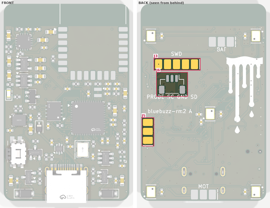
Every part on the board, why it was chosen, what it was chosen over, and the numbers behind its value, with the
datasheet pages and schematic blocks it comes from. Rev A, 28 × 44 mm, 6 layers, 109 components. Written 2026-10-18 from
scripts/circuit.py, bom/parts.yaml, the part audits in design/parts/ and
design/decisions.md.
Each block has three kinds of picture. Schematic
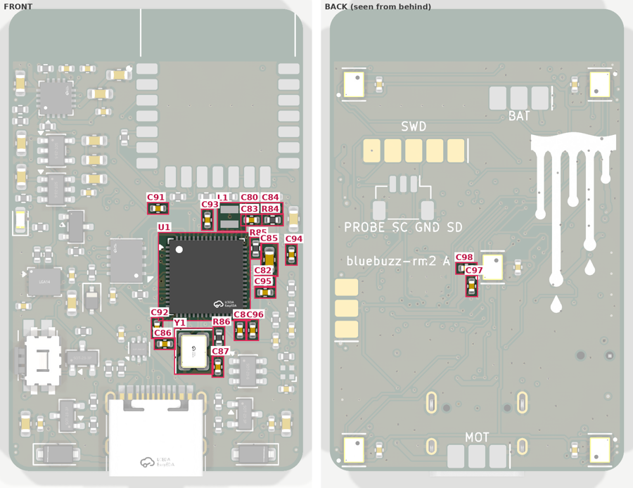
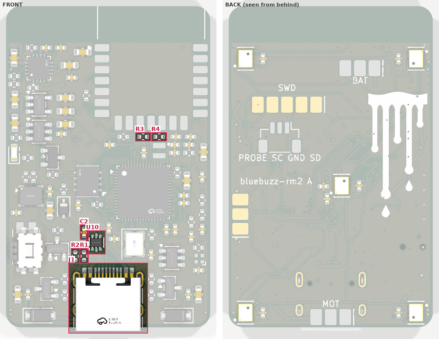
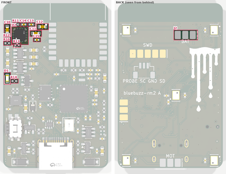
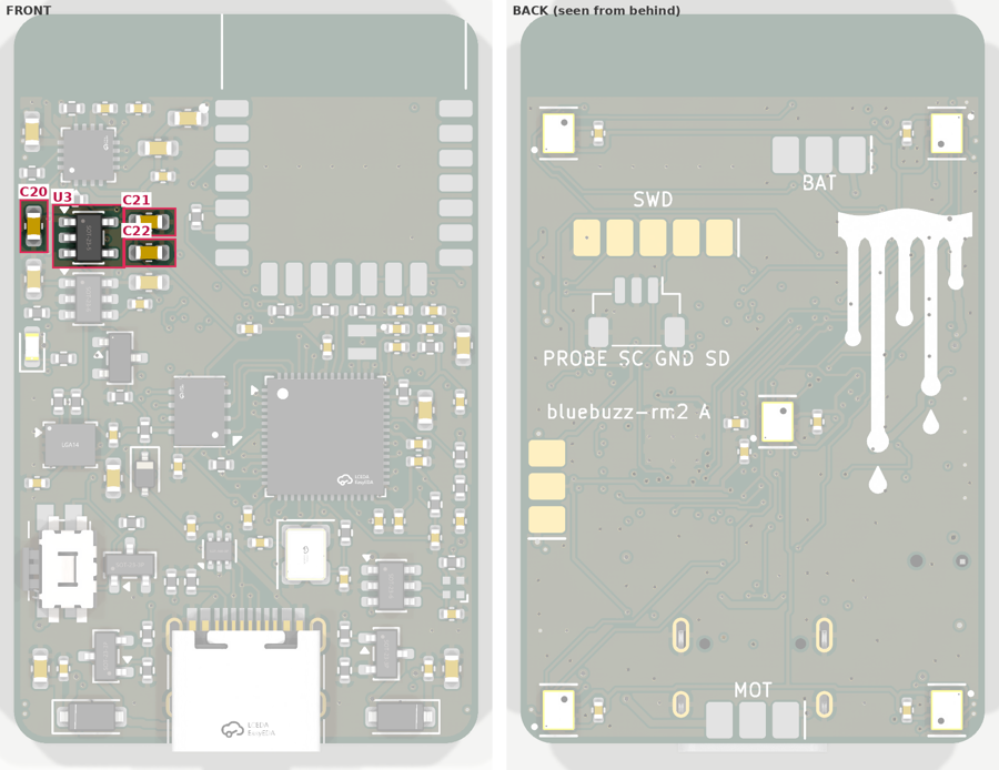
is the block as drawn in the generated sheet. Board shows where its parts sit, front and back (the back is
seen from behind, so it is mirrored left to right). Datasheet is the page a choice or value comes from.
Click any picture to see it full size, and click a datasheet caption to open the PDF at that page.
Overview
The board is a Bluetooth vibrator controller that is cast into a soft elastomer body. The parts were picked around four
requirements:
Bluetooth Classic audio (A2DP sink) and USB audio. This drove the RP2350A plus the Raspberry Pi Radio Module 2
(CYW43439), in place of the nRF52840 of the first board, which is BLE only. The Pico SDK supports this pairing directly.
No rework after casting. Every value follows a datasheet's reference circuit where one exists. Each
part has an audit in design/parts/. The board can be tested bare through pogo pads and USB.
Small, one connector. USB-C is the only connector. Battery, motors, SWD and test points are SMT pad rows on the back.
Passives are 0402, or 0603 where 1 µF and above needs it.
JLC assembly at quantity 5. Each part is an LCSC stock part where one exists, a JLC basic part where a choice
allowed it, and in stock in quantity. Two parts are consigned: the RM2, which is sold only through Raspberry Pi resellers,
and the Abracon core inductor, of which JLC had 3.
Power tree
VSYS is the charger's power-path output. When USB is present it is held at 4.4 V; otherwise
it is the cell through about 50–100 mΩ. Everything that can take the cell's voltage directly does, namely the motors, the radio and the LED.
That keeps the 500 mA LDO for the logic. When the LDO is off, the board is off: only the charger, the charge LED and the battery
divider still draw, about 10–15 µA in total.
RP2350 pin use
GPIO
Net
Goes to
2, 3
WL_DATA, WL_CLK
RM2 gSPI (pads 5/6/10, 3)
4
SENS_EN
U5 ON (sensor rail)
6, 7
SDA, SCL
I2C1 → IMU
8
BTN
Q3 drain (button, active low)
9
PG_N
charger /PGOOD (USB present)
10–12
TAC_SCK/SDI/SDO
SPI1 → all five DPS368
0, 14–16, 20
TAC_CS1–5
one chip select per sensor
13, 17
MOTOR1/2_PWM
gate resistors R40/R42 → Q1/Q2 (bottom pin row, toward the gates; PWM slices 6B and 0B)
5, 18
IMU_INT1/2
IMU interrupts (INT1 beside SDA/SCL, on the IMU's side)
19
PWR_HOLD
D5 → LDO EN (power latch)
22
LED_STAT
R62 → D2 DIN (pin 34, the side facing the LED)
27, 25
WL_ON, WL_CS
RM2 pads 12+13, 9 (WL_ON on the right-column pin nearest its pads)
26 (ADC0)
VBAT_SENSE
1 M / 1 M divider
1, 21, 23, 24, 28, 29
free (24 GPIOs used of 30)
Rails
Rail
Range
Source → loads
VBUS
5 V (5.5 max)
USB-C → U10 → charger IN; D6 → power latch
VBAT
3.0–4.2 V
cell ↔ charger BAT; battery divider
VSYS
3.0–4.4 V
charger OUT → LDO, RM2 Vin, motors, U11/LED, D1, SW1
3V3_SYS
3.3 V ±1 %
U3 → RP2350, flash, RM2 VDDIO, IMU, U5
1V1
1.1 V
RP2350's own buck via L1 → DVDD
3V3_SENS
3.3 V, switched
U5 → the five DPS368
LED_VDD
VSYS, switched
U11 → D2
3V3A, VREG_AVDD
3.3 V, filtered
10 Ω / 1 µF → ADC; 33 Ω / 4.7 µF → regulator
Current budget
At 10 % vibration duty: motors 2 × 0.2 A × 10 % = 40 mA (18 mA with the 0.09 A motors), RP2350 and
flash ≈ 30 mA, RM2 streaming A2DP ≈ 40 mA, everything else ≈ 5 mA, about 115 mA in total. A cell of ≥ 700 mAh gives 6 h,
and about 500 mAh gives 4 h. At the 500 mA charge rate a 700 mAh cell charges in about 1.7 h, inside the 6 h safety timer. The peak
VSYS draw is about 1 A: two motors plus a radio TX burst plus the LDO.
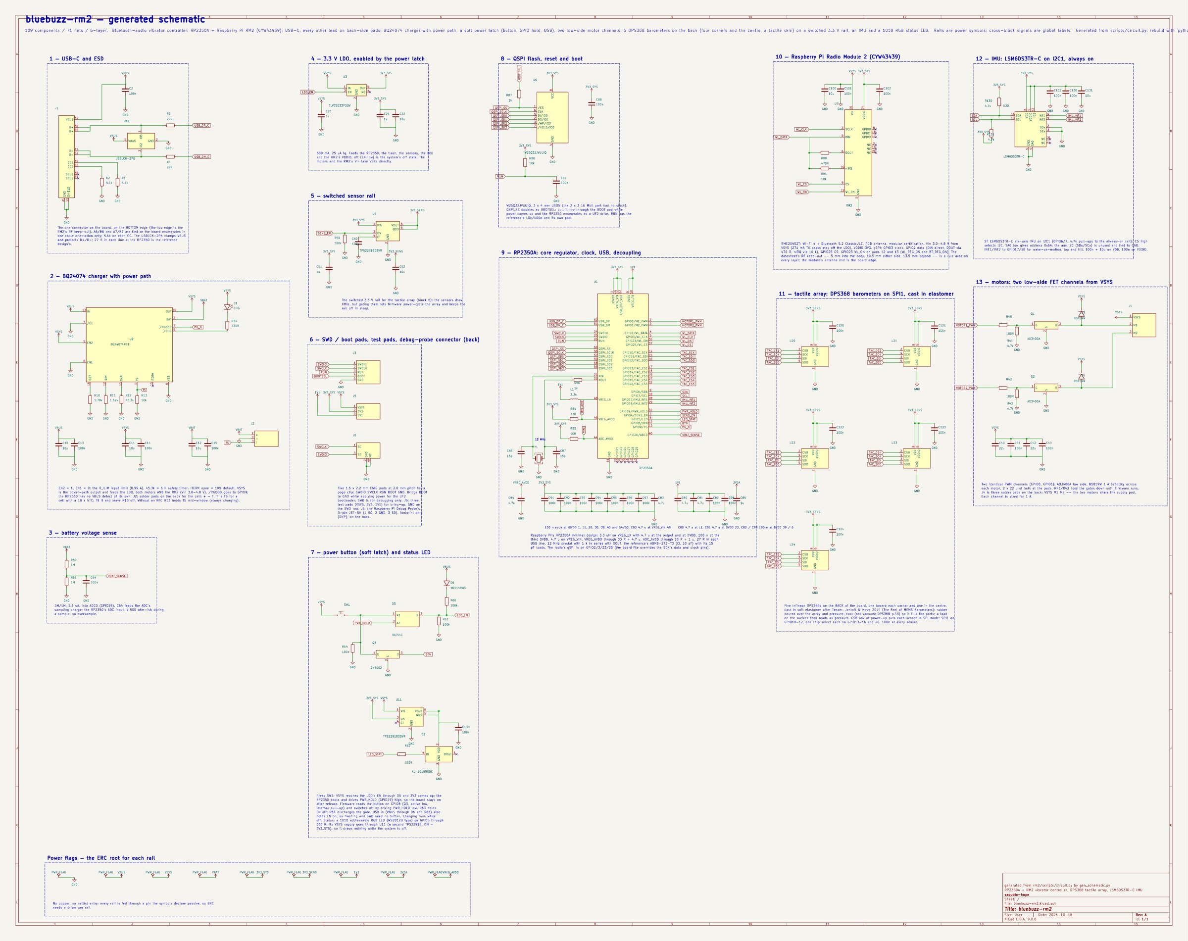
Schematic — the whole sheet. The numbered blocks are the sections below.
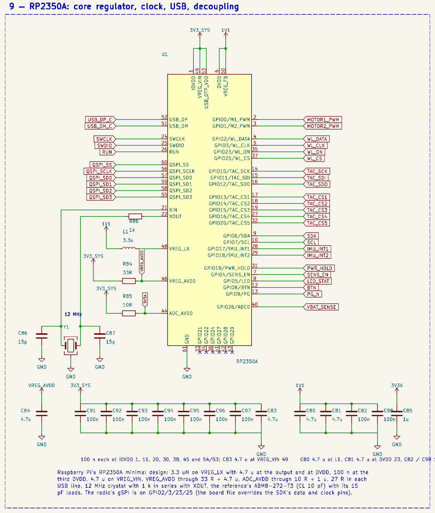
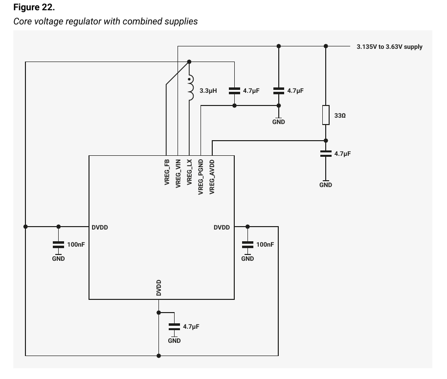
Block 9RP2350A host: core regulator, crystal, decoupling, USB
Ref
Part
Value / MPN
LCSC
Why
U1
MCU
RP2350A, QFN-60 7 × 7
C42411118
The RM2 works only with Raspberry Pi
microcontrollers. Of those, the RP2350 has 520 KB SRAM and Cortex-M33 cores with FPU and DSP, which suits BTstack plus SBC decoding. The A variant
(30 GPIO, 7 × 7 mm) rather than the B (48 GPIO, 10 × 10 mm): 24 GPIOs are used. $1.29, 6,240 in stock.
L1
Core buck inductor
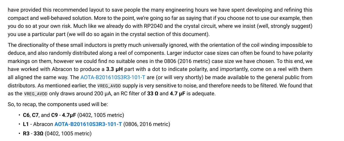
3.3 µH, Abracon AOTA-B201610S3R3-101-T (0806)
consigned
The
reference design's own part. Abracon made it with a polarity dot, all aligned on the reel, because the regulator is sensitive
to the coil's orientation. 2.1 A, 115 mΩ. JLC had 3 in stock, so ≥ 6 are bought from Digi-Key or Mouser and consigned. The Sunlord
MPL2016S3R3MHT (C98336) fits the same land as a fallback, but it has no dot.
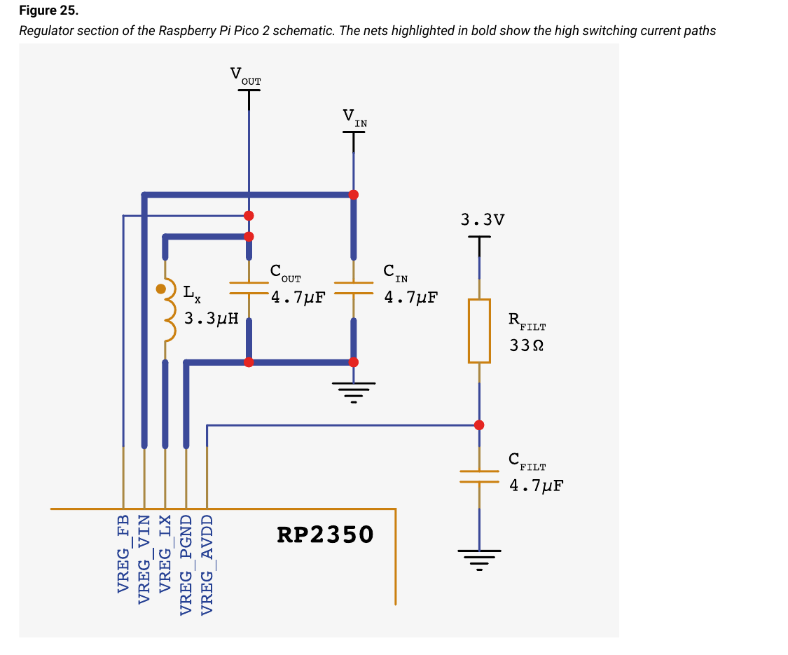
C80, C83
Buck COUT, CIN
4.7 µF X5R 10 V 0402
C23733
As in the datasheet's Figure 25, on Raspberry Pi's own
small-pad 0402 land and at the reference positions. The 10 V parts keep more capacitance at 3.3 V than the reference's 6.3 V ones (≈ 2.1–2.8 µF effective).
R84, C84
VREG_AVDD filter
33 Ω + 4.7 µF
C25105, C23733
The datasheet says this RC filter is required
("must be RC filtered"). VREG_AVDD draws about 200 µA, so the corner is about 1.9 kHz with only a 7 mV drop.
C81, C82, C98
DVDD (1.1 V)
4.7 µF at pin 23; 100 nF at pins 39 and 6
C23733, C1525
Datasheet
§6.1.3: 100 nF at the two DVDD pins nearest the regulator, and 4.7 µF at the far one. Each sits at the end of a 1V1 spoke from the ring under the chip
(see the layout rule below): C82 beside the E spoke's via, C81 on the back under the S spoke's via (the crystal is closer to the chip than on the
minimal board), C98 on the back off the ring's W via, behind pin 6.
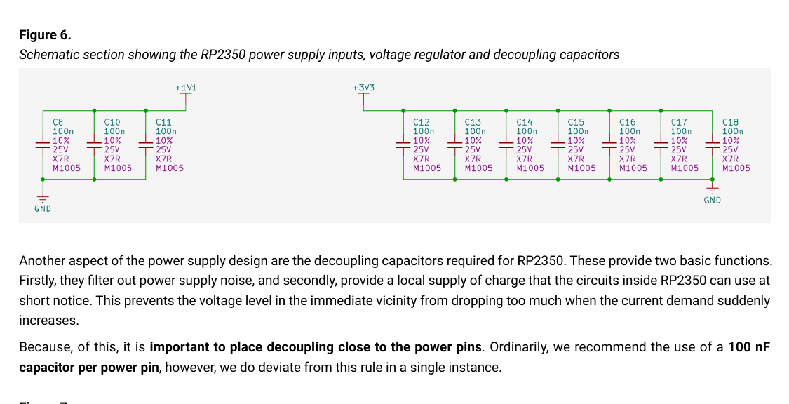
C91–C97
IOVDD, QSPI_IOVDD, USB_OTP_VDD
7 × 100 nF X7R
C1525
The guide asks for one per power pin; pins 53 and 54
share one cap (C93), at the reference position. C97 is on the back behind pin 11, where the front lane is the escape for pins 2–13; C91 is on the back under its own via beside pin 1, where the QSPI lines fan out on the front.
R85, C85
ADC_AVDD filter
10 Ω + 1 µF 0603
C25077, C15849
Stricter than either document asks.
This keeps the motor PWM off the ADC reference that the battery gauge relies on.
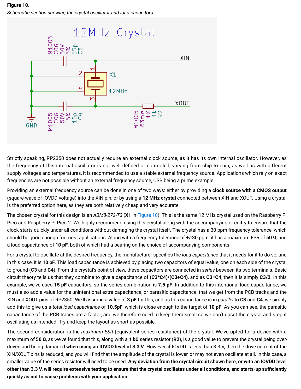
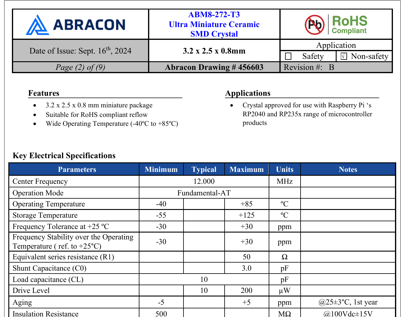
Y1
Crystal
12 MHz Abracon ABM8-272-T3, 3225
C20625731
The crystal of the reference design, which is the
only validated circuit. CL 10 pF, ESR ≤ 50 Ω. The first pick (TXM12M, CL 12 pF, 120 Ω) was dropped: its datasheet could not be
obtained, and the guide says any deviation needs temperature testing.
C86, C87
Load caps
15 pF C0G
C1548
15 ∥ 15 pF in series = 7.5 pF, plus 3 pF stray = 10.5 pF ≈ CL 10 pF.
R86
XOUT series
1 kΩ
C11702
Limits the drive level at IOVDD 3.3 V ("tuned for 3.3 V operation").
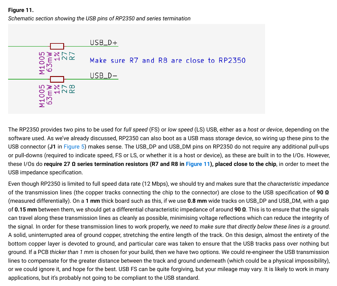
R3, R4
USB series
27 Ω
C25100
Required by the RP2350 and placed at the chip; together with the driver they meet the USB 28–44 Ω source impedance.
No external pull-ups: the RP2350 has them built in.
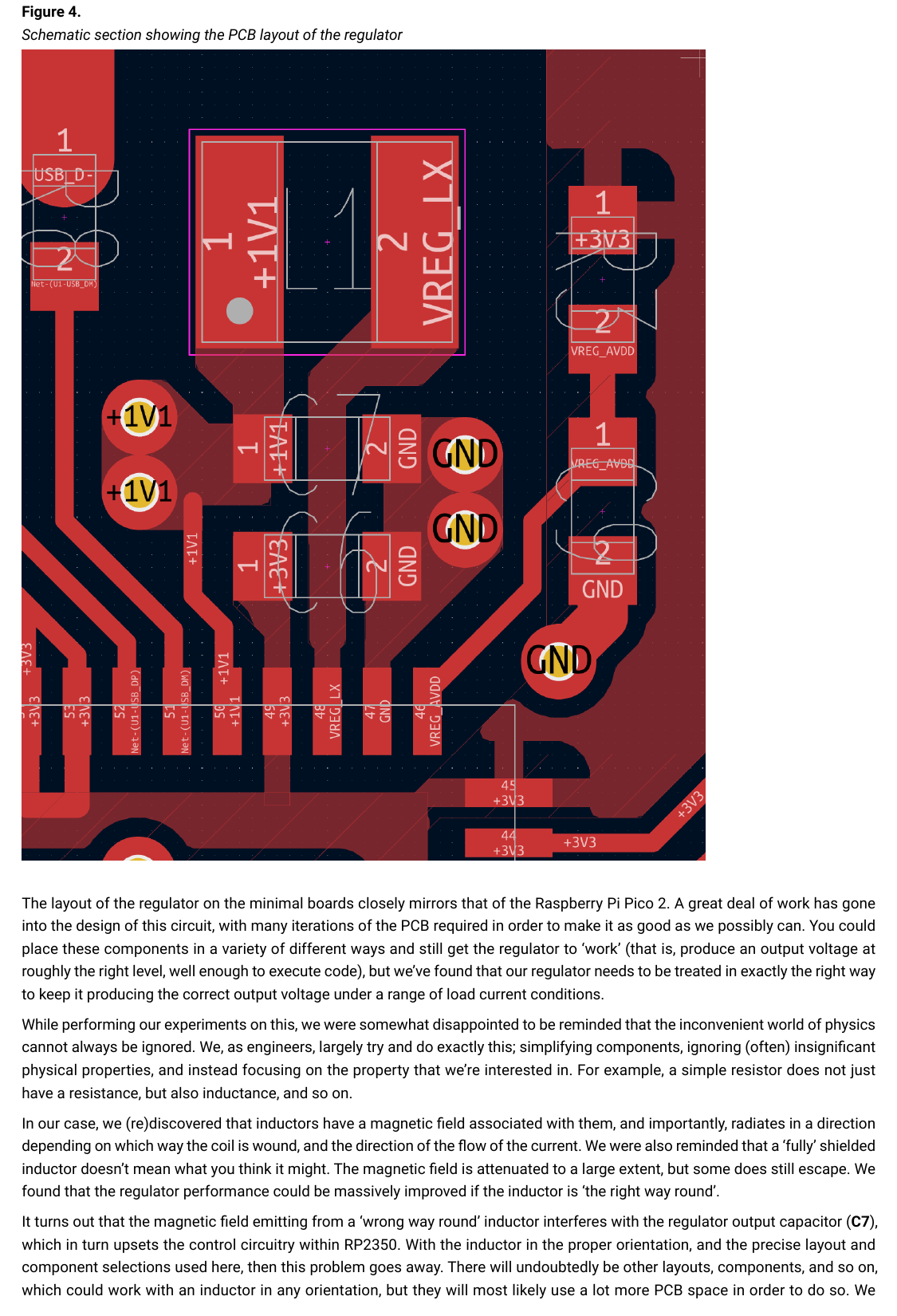
Layout rule: the RP2350's power copper is Raspberry Pi's own. scripts/rp2350_block.py reads the RP2350A
minimal board's KiCad file (design/reference/) and lays its power block relative to U1, locked, before the autorouter runs:
Under the chip, on top: a 1V1 ring around the GND pad, inside a 3V3 band that reaches every IOVDD pad.
1V1 spokes: four 0.6 mm spokes (on In2 here) from the ring to the DVDD pins and to COUT.
Regulator: the regulator's parts at the reference positions and rotations, and its small high-current zones (LX, 1V1, CIN's 3V3, PGND).
PGND reaches the GND planes only through its pair of adjacent vias: those pads get no via-in-pad, and a moat keeps the top GND pour out.
The In1 GND plane is cut away under the LX node (datasheet §6.3.8.1, Fig. 27). L1 sits at the reference rotation, so its dot lands where the
reference puts it. The audit checks all of this on every build.
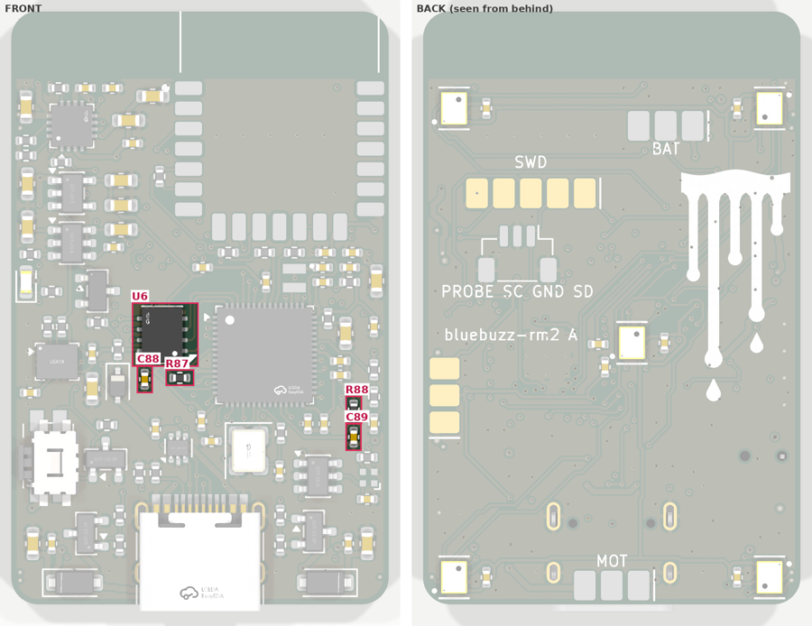
Schematic — block 9.Board — the chip at the centre, with L1 and the
regulator caps above it, the crystal below it, and C97/C98 on the back.
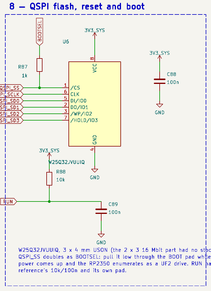
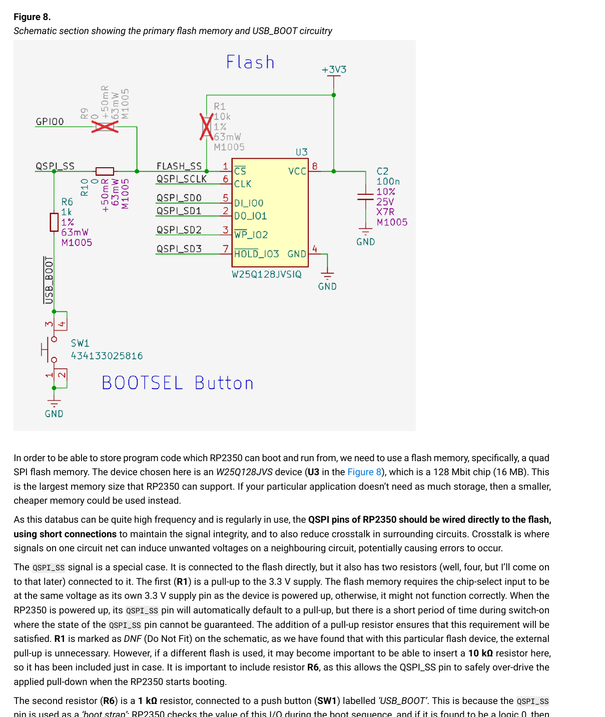
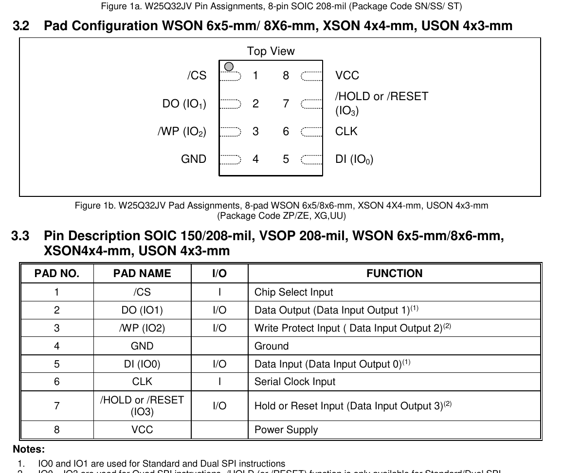
The W25Q family is the one the RP2350 boot ROM
and the SDK's boot2 are written for. The 16 Mbit 2 × 3 USON of the other RP2350 boards here had no stock anywhere at LCSC, and the SOIC-8 is 5.3 × 5.3 mm.
The "Q" suffix fixes QE = 1, which quad mode on /WP and /HOLD needs. It runs at 75 MHz quad I/O (≤ 133 MHz).
C88
Decoupling
100 nF
C1525
At pin 8.
R87
BOOTSEL strap
1 kΩ QSPI_SS → BOOT pad
C11702
No BOOTSEL button. Bridge the BOOT pogo pad to GND while powering up to get
the UF2 bootloader; firmware can also reboot into it. The 1 kΩ lets QSPI_SS overdrive the strap once the chip runs (3.3 mA).
R88, C89
RUN
10 kΩ + 100 nF
C25744, C1525
A defined pull-up, plus about 1 ms of reset hold-off after 3.3 V rises.
RUN also goes to a pogo pad, so there is no reset button.
Schematic — block 8.Board — the flash, turned 180° so that SS, SD1 and SD2 face the QSPI pins.
Datasheet —
the reference flash and USB_BOOT circuit, with the 1 kΩ strap and the 10 kΩ pull-up that is not fitted. Hardware design with RP2350 p.10Datasheet —
USON 4 × 3 pad assignment. W25Q32JV p.5
Block 10Raspberry Pi Radio Module 2
Ref
Part
Value / MPN
LCSC
Why
U7
Radio module
RM2, RMC20452T (CYW43439)
consigned
Wi-Fi 4 plus Bluetooth 5.2 Classic and LE in a certified,
shielded module with a PCB antenna. It is the Pico 2 W's radio, so the SDK's CYW43 driver and BTstack (A2DP) work unchanged. $4 RRP;
sold through Raspberry Pi resellers only, so it is consigned or hand-soldered.
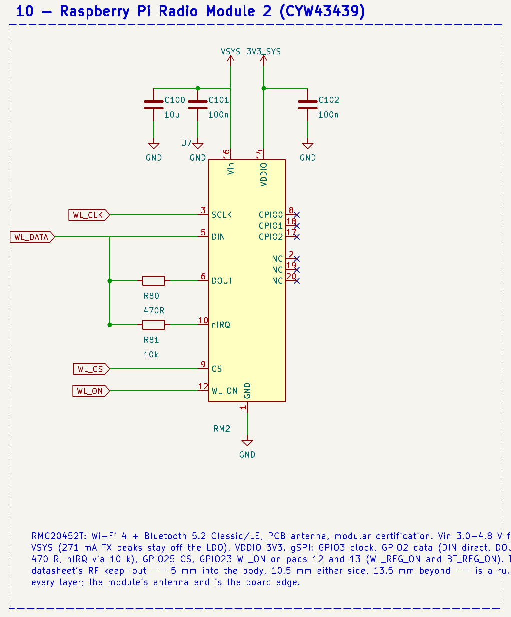
R80
DOUT → DATA
470 Ω
C25117
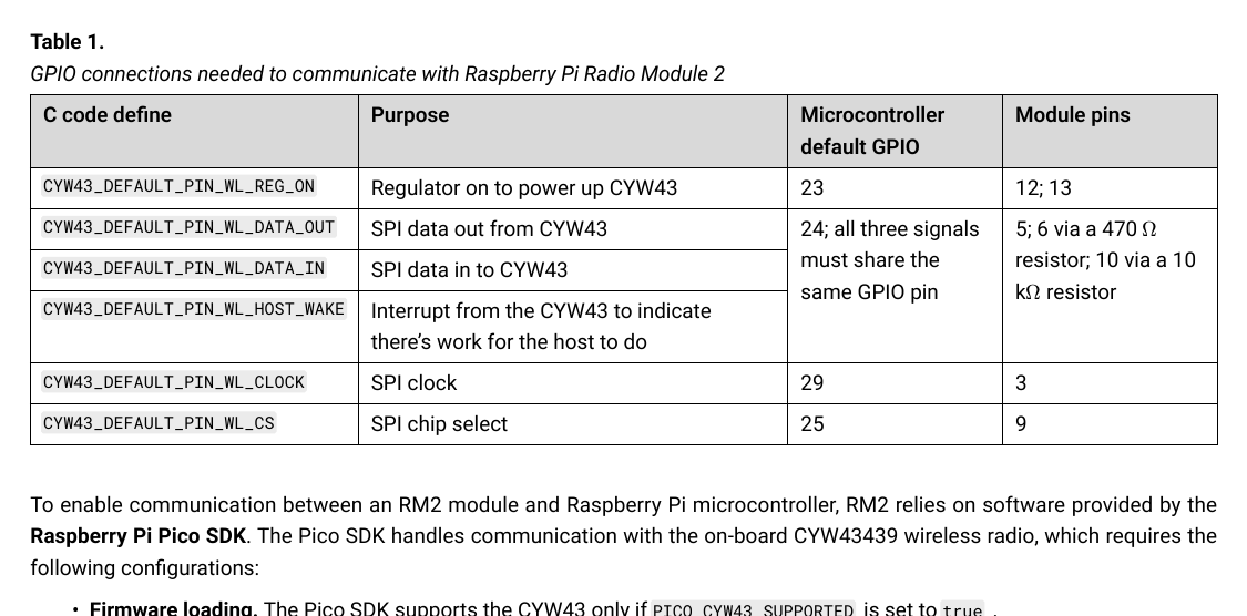
Required by the datasheet (Table 1): DATA_OUT, DATA_IN and HOST_WAKE share one GPIO.
R81
nIRQ → DATA
10 kΩ
C25744
Required by the same table.
C100, C101
Vin
10 µF + 100 nF
C19702, C1525
The module has its own regulators, and the datasheet asks for nothing.
These cover its TX bursts. C100 sits 3 mm from pad 16's column.
C102
VDDIO
100 nF
C1525
At pad 14.
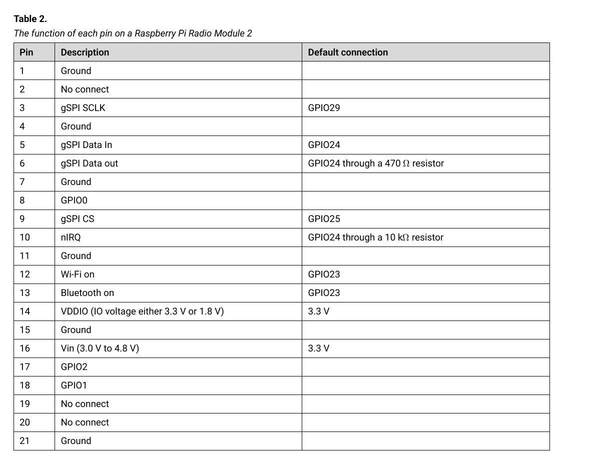
Vin from VSYS, not the LDO. TX peaks of 271 mA (budget 350 mA) would leave too little of the TLV75533's 500 mA. Vin is
rated 3.0–4.8 V, with RF degrading below 3.2 V, so firmware cuts off at a 3.5 V cell.
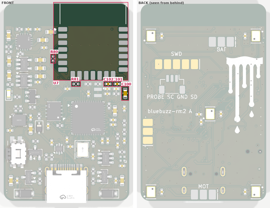
gSPI on GPIO2/3 instead of the Pico W's 24/29. The module's DIN/DOUT/SCLK pads face the RP2350's top-left, where GPIO2 and 3 are.
The datasheet allows any pins ("You can change the default GPIO assignments at build time"). The board header overrides
CYW43_DEFAULT_PIN_WL_DATA_*, _WL_CLOCK and _WL_REG_ON: WL_ON is on GPIO27 (pin 41), the right-column
pin nearest the module's pads 12/13, because the RP2350's reference regulator block now sits under those pads. CS (25) stays at the default.
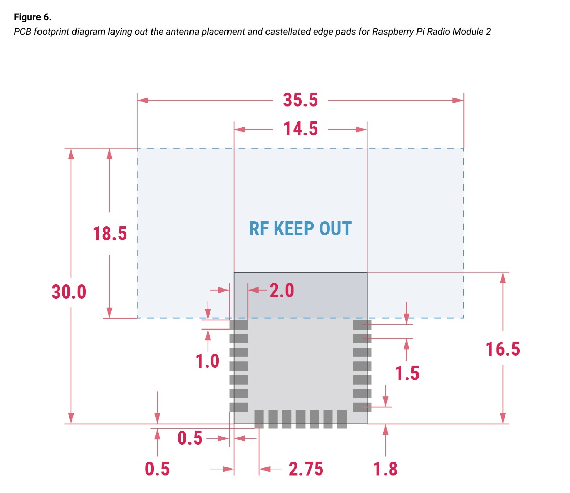
RF keep-out: no copper on any layer within 5 mm of the antenna end, across the full board width. The body will detune the antenna somewhat;
measure range in air and when cast before fixing the body's shape.
Schematic — block 10.Board — top-right, with the antenna on the top edge.
Datasheet —
the shared DATA pin and its 470 Ω / 10 kΩ resistors. RM2 datasheet p.5, Table 1Datasheet —
footprint and RF keep-out. An audit found the side pads 0.2 mm off this drawing; they are now corrected. RM2 datasheet p.9, Fig. 6Datasheet —
pin functions: VDDIO 3.3 V, Vin 3.0–4.8 V. RM2 datasheet p.10, Table 2
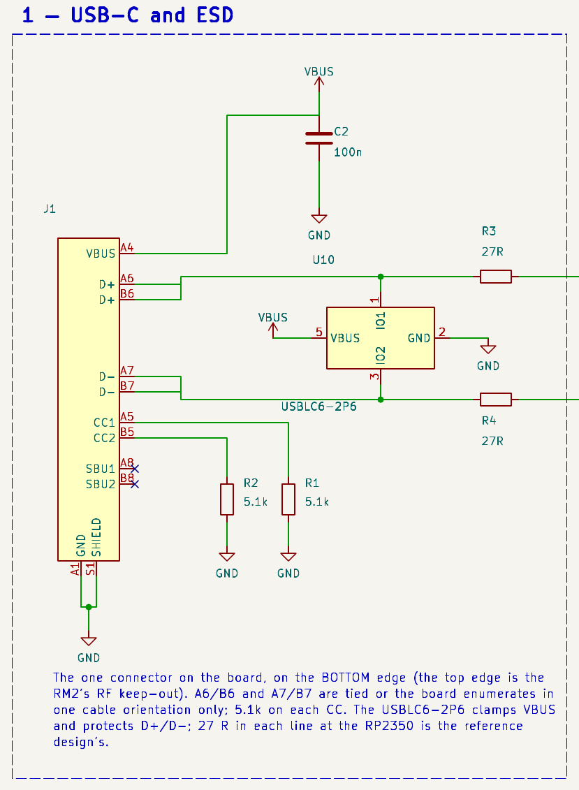
Block 1USB-C and ESD
Ref
Part
Value / MPN
LCSC
Why
J1
Receptacle
HRO TYPE-C-31-M-12, 16-pin USB 2.0
C165948
The same part as the first board, and a
JLC staple. The 16-pin type has no SuperSpeed contacts. It sits centred on the bottom edge, mouth flush; the top edge is the antenna keep-out.
A6/B6 and A7/B7 are tied so either plug orientation works.
R1, R2
CC pull-downs
5.1 kΩ each
C25905
The Type-C Rd for a sink, one per CC pin. The source then supplies 5 V even into a dead board,
so a flat cell can charge.
U10
ESD array
ST USBLC6-2P6, SOT-666
C15999
The usual low-capacitance (≈ 3.5 pF) rail-to-rail array with a VBUS TVS. The
USB-C is the only user-touched metal. D+ passes through pins 1→6 and D− through 3→4.
C2
VBUS HF cap
100 nF X7R 16 V
C1525
Gives the array's VBUS node a local return for the first nanoseconds of a strike.
There is no PD controller and no CC sensing. The charger takes up to 1 A from any 5 V source; phone chargers and
Type-C sources advertising 1.5 A or more cover that. The shell goes straight to GND as the discharge path. There is no surge protection beyond ESD,
consistent with a personal device with no formal compliance.
Schematic — block 1.Board — bottom edge, with the ESD array above-left of the receptacle;
R3/R4 sit at the RP2350.
Datasheets missing: the TYPE-C-31-M-12 drawing and the USBLC6-2 datasheet could not be downloaded (LCSC and ST block
the fetcher). The pin maps come from KiCad's footprint for this exact part and from ST's standard SOT-666 pinout. Please attach both if you can.
Block 2BQ24074 charger with power path
Ref
Part
Value / MPN
LCSC
Why
U2
Charger
TI BQ24074RGTR, VQFN-16 3 × 3
C54313
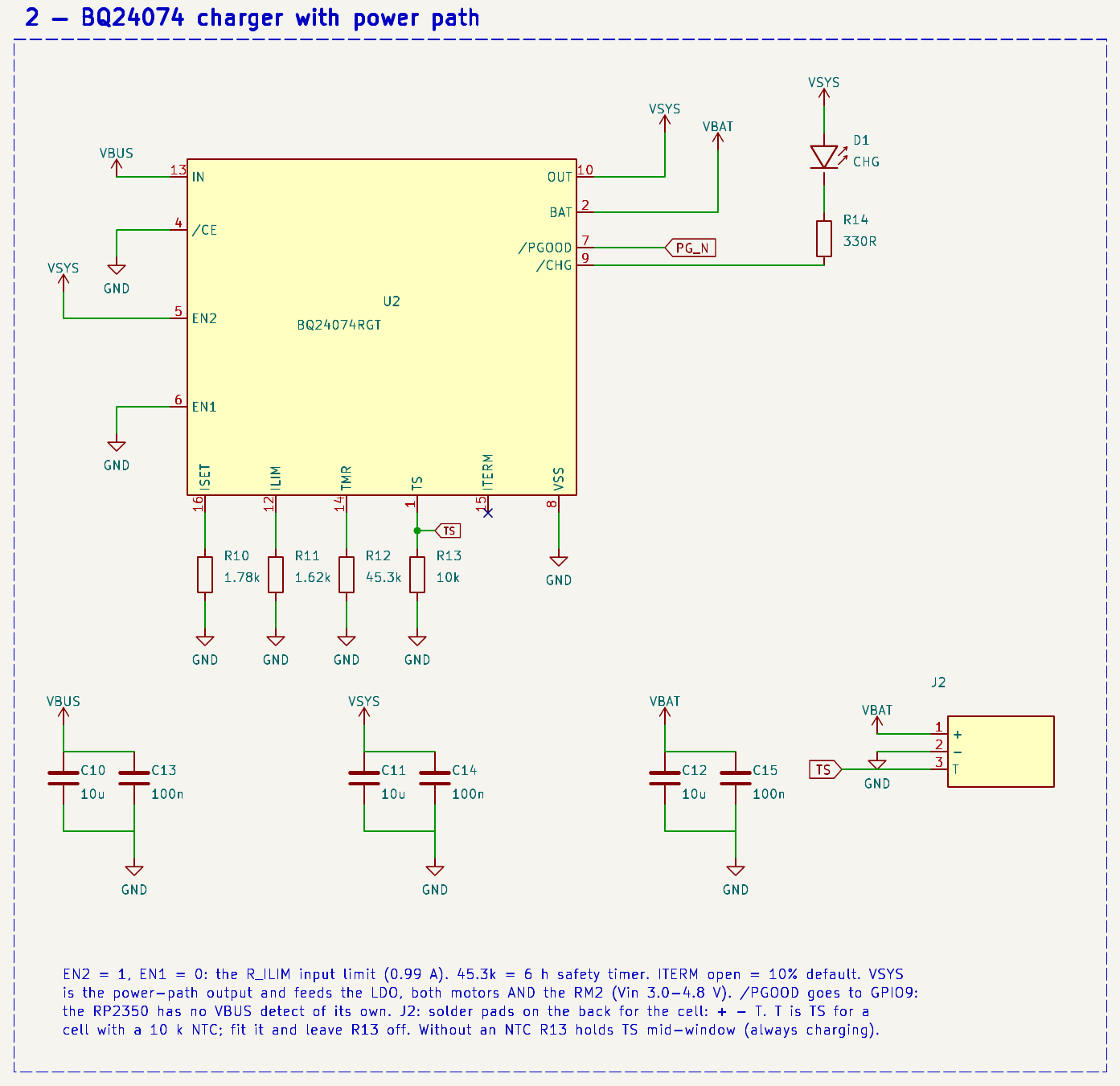
Power path: the system runs from USB with a flat or missing cell,
and charge termination is not confused by the system load (simple chargers like the MCP73831 or TP4056 put the load on the cell). Other reasons: 28 V input rating, 10.5 V OVP,
a programmable input limit and timer, /PGOOD and /CHG outputs. Already proven on the bike-tracker board.
R10
ISET
1.78 kΩ 1 %
C113478
ICHG = 890 / 1780 = 500 mA (448–548 mA), 0.7 C for a 700 mAh cell.
Holds TS mid-window (0.75 V; trip points 0.3 and 2.1 V), so charging is always allowed. Leave it off if the
cell has a 10 k NTC on the BAT row's T pad; that gives a 0–50 °C charge window.
C10, C13
IN
10 µF + 100 nF
C19702, C1525
Datasheet 1–10 µF. About 6 µF after DC bias, under the Type-C sink limit.
C11, C14
OUT (VSYS)
10 µF + 100 nF
C19702, C1525
Datasheet 4.7–47 µF; about 30 µF effective on the rail with the motor bulk caps.
C12, C15
BAT
10 µF + 100 nF
C19702, C1525
Datasheet 4.7–47 µF.
D1, R14
Charge LED
Everlight 0603 green + 330 Ω
C2986059, C25104
Driven from VSYS by /CHG, so it lights while the system is off. A few mA.
J2
BAT pads
3 pads, back: + − T
—
Solder pads for the cell lead. T is TS, for an NTC cell.
EN1 = GND, EN2 = VSYS selects the RILIM input limit. EN2 was on 3V3; it moved to VSYS when the power latch was added, so that
a switched-off system still charges at the full rate. TI's standalone example ties EN2 to OUT the same way. /CE is tied low.
/PGOOD → GPIO9 tells the firmware that USB is present; the RP2350 has no VBUS detect. There is no external pull-up, so firmware
must enable the internal one.
Thermal: the worst case is a cold cell charging at a 5.5 V input with the system busy: 1.6 W, TJ ≈ 116 °C on a JEDEC board. The chip only
throttles the charge current at 125 °C. Four thermal vias in the PowerPad tie it to both GND planes.
Schematic — block 2.Board — top-left, with the set resistors in line with their pins.
The BAT pads are on the back.
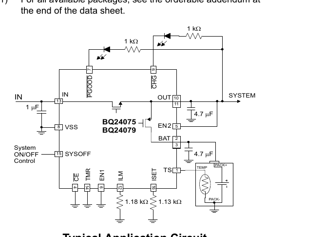
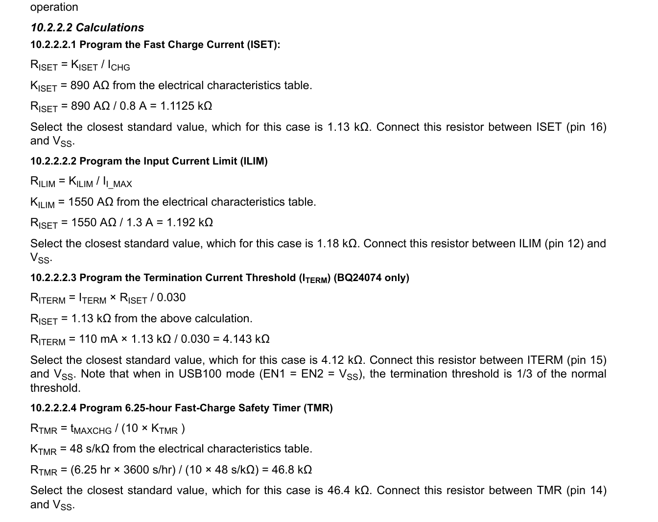
Datasheet —
the typical application circuit. BQ24074 p.1Datasheet —
TI's worked ISET, ILIM, ITERM and TMR calculations, the same equations used above. BQ24074 p.34
Block 43.3 V LDO
Ref
Part
Value / MPN
LCSC
Why
U3
LDO
TI TLV75533PDBVR, SOT-23-5
C404027
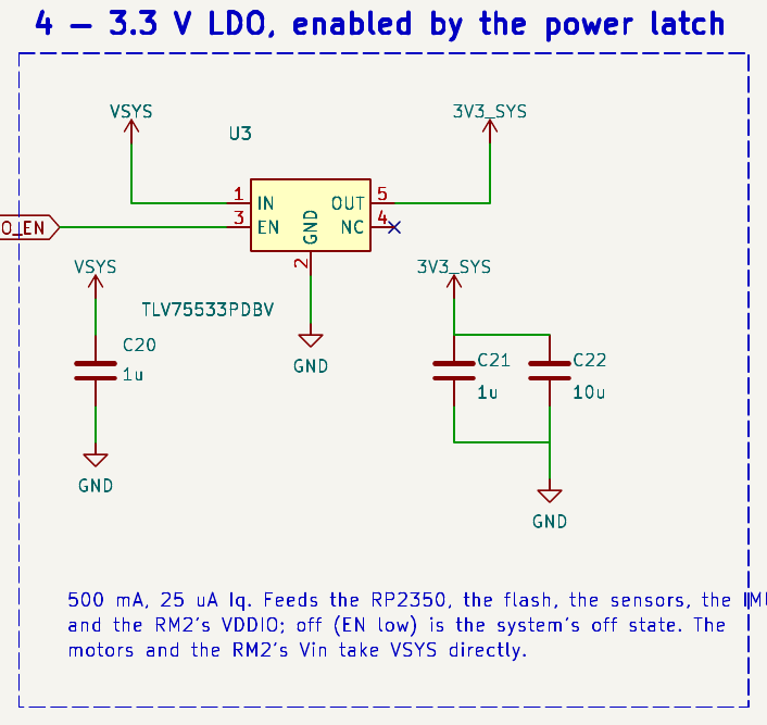
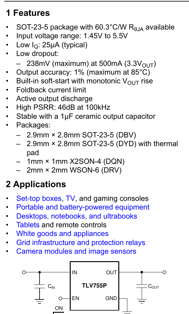
500 mA, 25 µA quiescent, 238 mV max dropout at 500 mA, and stable with 1 µF ceramics.
Its enable input is what the power latch drives: off draws about 0.1 µA. A buck-boost would hold 3.3 V down to an empty cell, but costs area and
quiescent current; firmware cuts off at 3.5 V instead.
C20
IN
1 µF 0603 X5R 50 V
C15849
Datasheet ≥ 1 µF (≥ 0.47 µF effective). A 50 V part loses under 10 % at 4.4 V.
C21, C22
OUT
1 µF + 10 µF
C15849, C19702
≥ 1 µF required. About 8 µF effective, plus about 28 µF across the whole 3V3 net.
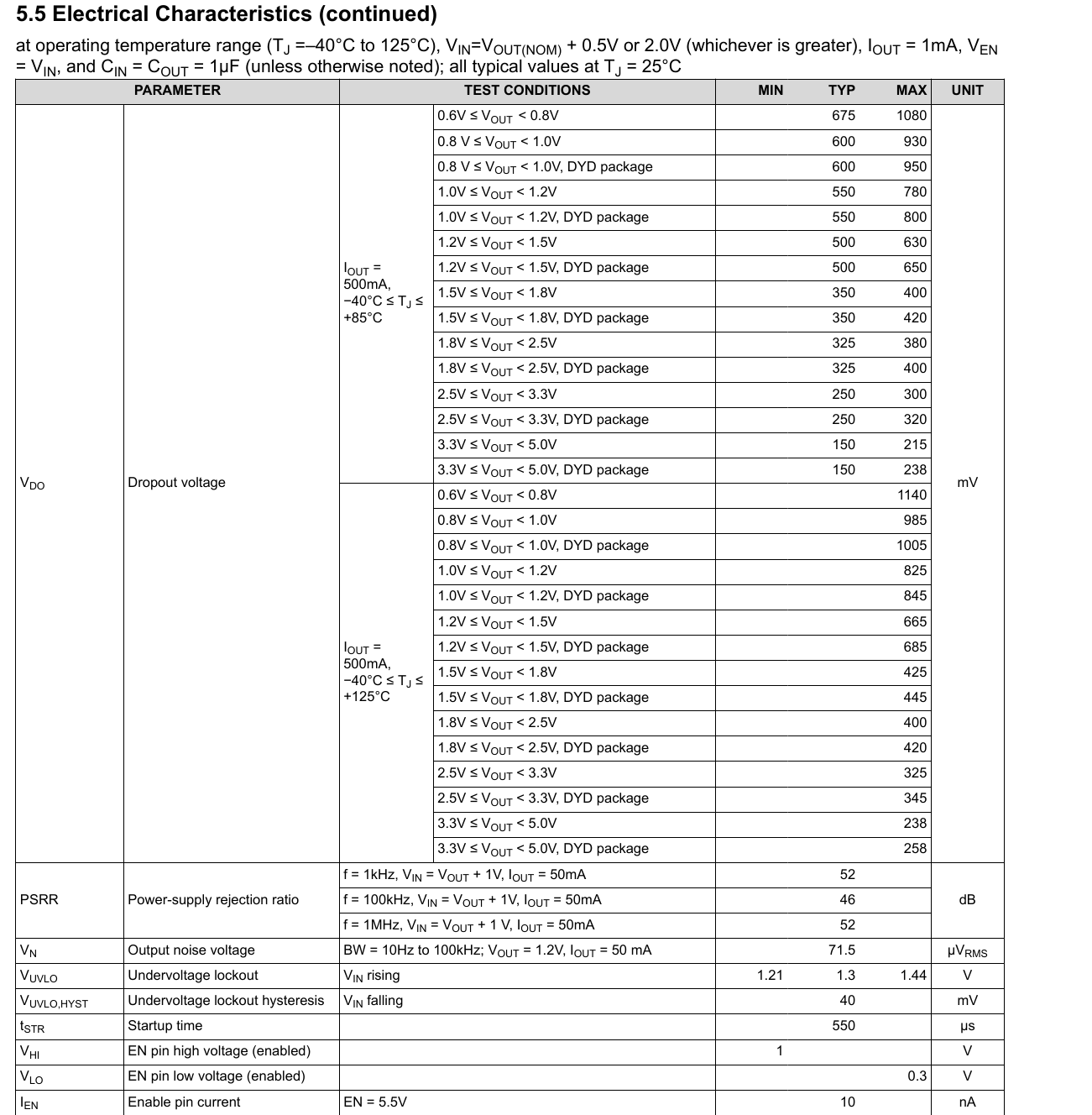
Dropout: it regulates down to VSYS ≈ 3.44 V at 250 mA. Below that, 3V3 tracks the cell minus about 75 mV, and the ADC reference falls with it.
That is why firmware shuts down at 3.5 V, measured while the reference is still good.
Heat: the worst case is (4.4 − 3.3) V × 250 mA = 0.28 W, which gives TJ 73–109 °C at 45 °C depending on the copper. No thermal pad on the DBV package,
so GND pin 2 is stitched into the planes.
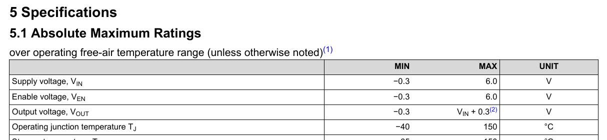
EN absolute maximum is 6.0 V. The latch puts VSYS − 0.3 V (≤ 4.1 V) on EN from the button, about 3 V from PWR_HOLD, and about 2.3 V from USB.
At the charger's 10.5 V OVP limit, the 2:1 USB divider still keeps EN under 6 V.
Schematic — block 4.Board — below the charger on the left.
Datasheet —
headline specs and the typical application circuit. TLV755P p.1Datasheet —
the 6.0 V absolute maximum on EN, which sizes the USB divider R66/R63. TLV755P p.4Datasheet —
dropout (3.3 V rows: 215 mV max at 85 °C), and EN VHI 1 V / VLO 0.3 V. TLV755P p.6
Block 7Power button (soft latch) and status LED
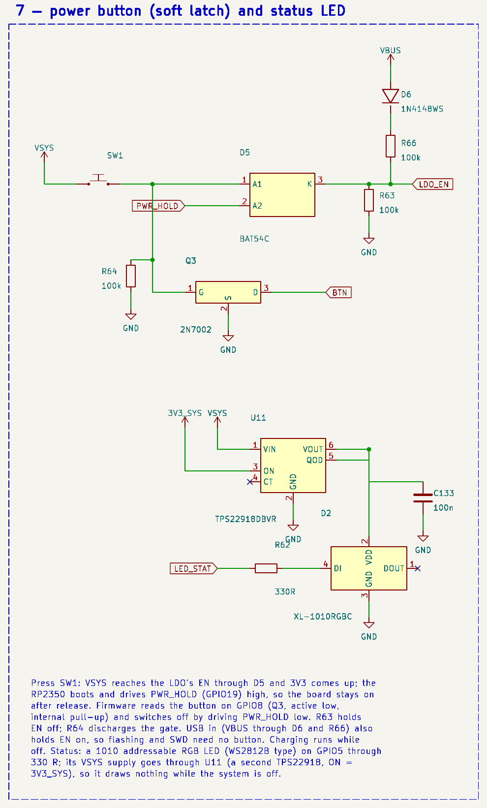
What was asked for: a momentary button that powers up the CPU, which then latches power on. The button stays readable, and the CPU can
switch itself off. USB power also keeps the board on (option 1).
Ref
Part
Value / MPN
LCSC
Why
SW1
Button
Panasonic EVQPUC02K, side-actuated
C79174
Its plunger stands 0.5 mm past the left edge, so it can be found and pressed through the rubber.
It is low profile, and the same part as the first board. A press puts VSYS on BTN_RAW.
D5
OR diode
BAT54C, common cathode
C37704
Two Schottky inputs in one SOT-23: BTN_RAW and PWR_HOLD (GPIO19) OR'd onto the LDO's EN. The
low VF keeps EN high from 3.3 V logic.
R63
EN pull-down
100 kΩ
C25741
Holds the LDO off when nothing drives EN.
D6, R66
USB → EN
1N4148WS + 100 kΩ
C2128, C25741
USB keeps the board on. Without it, a blank board or the UF2 bootloader (which never drives PWR_HOLD)
would lose power as soon as the button is released. With R63, R66 forms a 2:1 divider, so EN stays below 6 V even at the charger's 10.5 V OVP.
Q3, R64
Button read
2N7002 + 100 kΩ
C8545, C25741
The 4.4 V button node must not reach a GPIO, so an N-FET pulls GPIO8 (internal pull-up) low while
the button is pressed. R64 discharges the gate after release.
D2
Status LED
XL-1010RGBC-2812B-S, 1.0 × 1.0 mm WS2812B-type
C51900942
The 1010 addressable LED that was asked for, with full RGB
from one GPIO. It needs 3.5–5.5 V, so it runs from VSYS (≥ 3.5 V above the firmware cutoff). Its DI threshold of 0.7 × VDD ≤ 3.08 V is met by 3.3 V logic.
U11
LED supply switch
TPS22918DBVR, ON = 3V3_SYS
C131941
The LED idles at 0.35 mA, which would drain the cell while the board is off.
A second TPS22918 does the switching with one part already on the BOM, in place of a P-FET, an N-FET and a resistor.
R62, C133
DIN series, decoupling
330 Ω, 100 nF
C25104, C1525
The usual WS2812 series resistor, which damps ringing on DIN, and the LED's supply cap.
Sequence: a press puts VSYS on EN through D5, 3.3 V comes up and the RP2350 boots. Firmware drives GPIO19 high early in boot,
so the user holds the button only until that point. To switch off, firmware drives GPIO19 low (it can't while USB is in; it can still sleep and turn the LED and motors off).
The board is designed with no separate user button; SW1 is read on GPIO8 while the board runs.
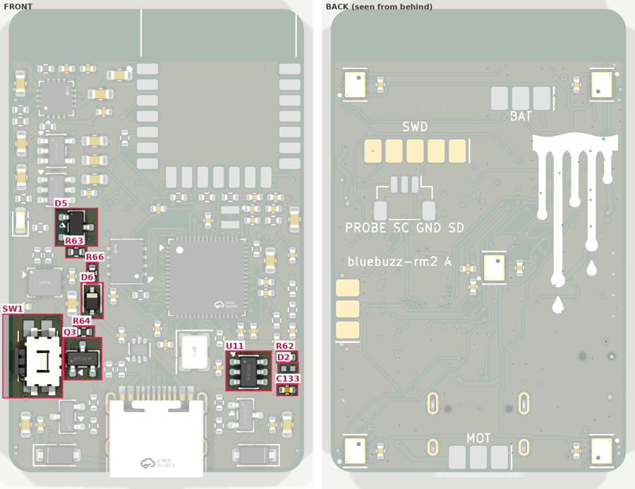
Schematic — block 7.Board — SW1 on the left edge with the latch parts between it and the chip;
the LED and U11 on the right edge.
Datasheet —
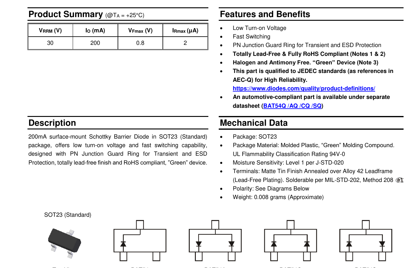
BAT54C: 30 V, 200 mA, common cathode (the third symbol). This is Diodes Inc.'s sheet; the BOM's BAT54C,215 is Nexperia's, with the same pinout. BAT54 p.1Datasheet —
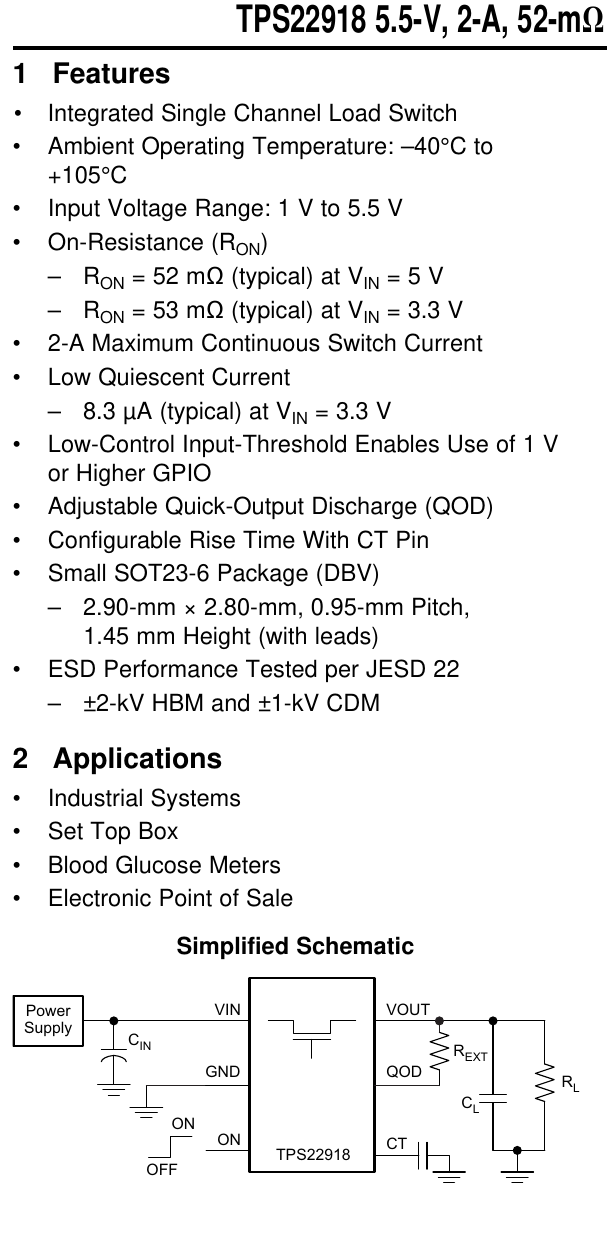
TPS22918: 1–5.5 V, 52 mΩ, quick output discharge. It is used here as U11, and again as U5 for the sensor rail. TPS22918 p.1
Datasheets missing: XL-1010RGBC-2812B-S (LCSC only), 2N7002, 1N4148WS and EVQPUC02K. The pinouts come from the LCSC/EasyEDA
footprints and the KiCad library, and the electrical needs here are far from the limits of any of these parts.
Block 3Battery voltage sense
Ref
Part
Value
LCSC
Why
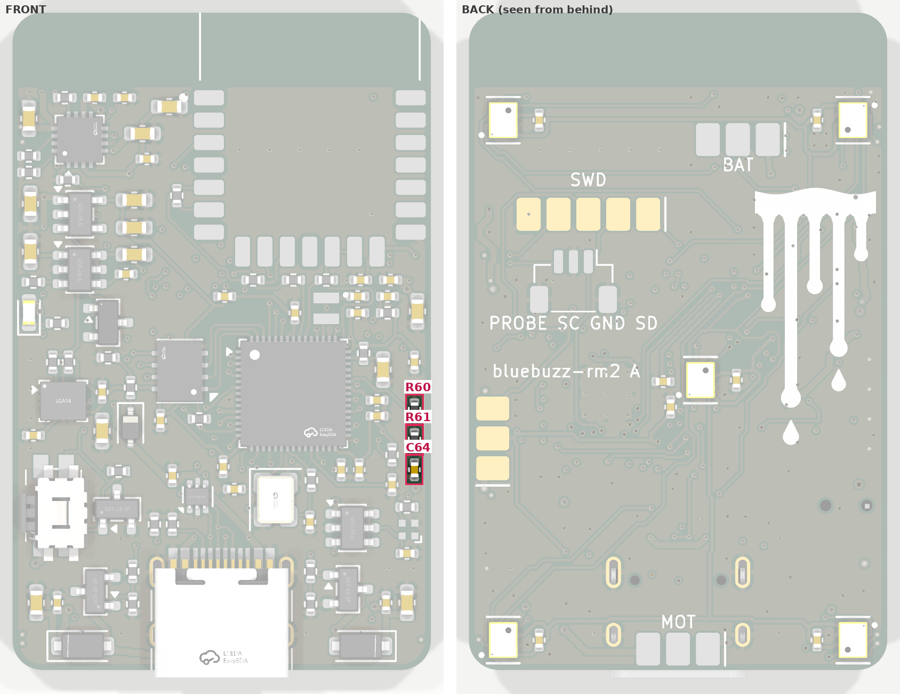
R60, R61
Divider
1 MΩ / 1 MΩ
C26083
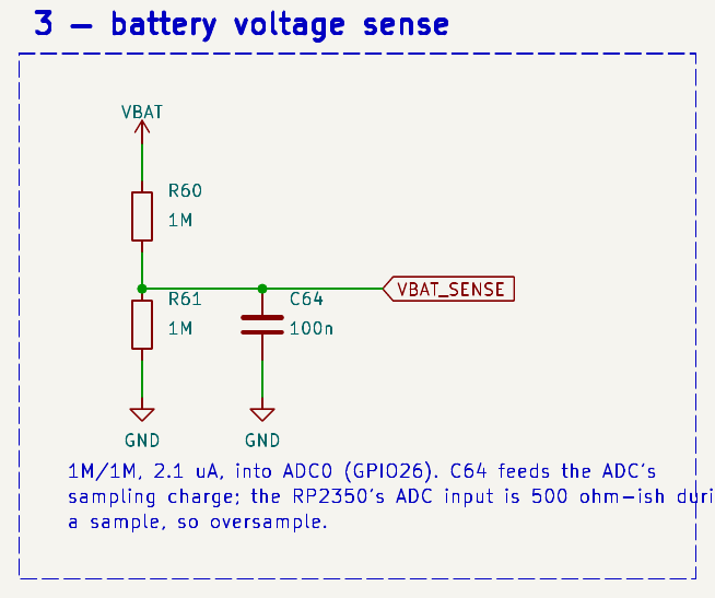
Puts 4.35 V at 2.18 V, under the ADC's 3.3 V range, while drawing only 2.1 µA from the cell all the time.
C64
Reservoir
100 nF
C1525
Without it, a 500 kΩ source into an ADC input of about 100 kΩ reads badly wrong. With it, each conversion dips the
node by only about 21 µV. Recovery time is 50 ms; a battery gauge at ≤ 1 S/s doesn't notice.
The ADC reference is 3V3, which falls in LDO dropout below about 3.4 V. The gauge reads a ratio and is trusted above about 3.5 V. The
1 µA worst-case pin leakage spec would allow a 24 % error on paper; real leakage is in the nA range. Calibrate once against a known cell voltage.
Schematic — block 3.Board — down the right edge, away from the buck inductor.
Block 5Switched sensor rail
Ref
Part
Value / MPN
LCSC
Why
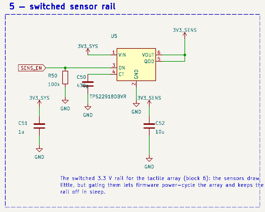
U5
Load switch
TI TPS22918DBVR, SOT-23-6
C131941
Turns the five barometers fully off in sleep (0.5 µA switch leakage).
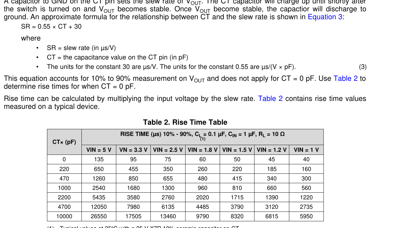
Each power-up is also a clean power-on reset, which the DPS368 needs to select SPI. It has an adjustable slew (CT) and quick output discharge.
C50
CT
470 pF C0G
C75274
Rise time ≈ 0.85–0.95 ms, inside the DPS368's 0.001–5 ms supply-ramp window. Inrush ≈ 30 mA instead of about 0.3 A.
Keep it under about 2.7 nF.
R50
ON pull-down
100 kΩ
C25741
The ON pin must not float while the RP2350 is in reset.
C51, C52
IN, OUT
1 µF, 10 µF
C15849, C19702
1 µF at VIN as recommended. 10 µF of bulk for the five sensors.
Firmware rule: park SCK, SDI and all five CS lines low before dropping SENS_EN, and keep them low until the rail is back.
A line left high back-powers the sensors into the switch's 25 Ω discharge path.
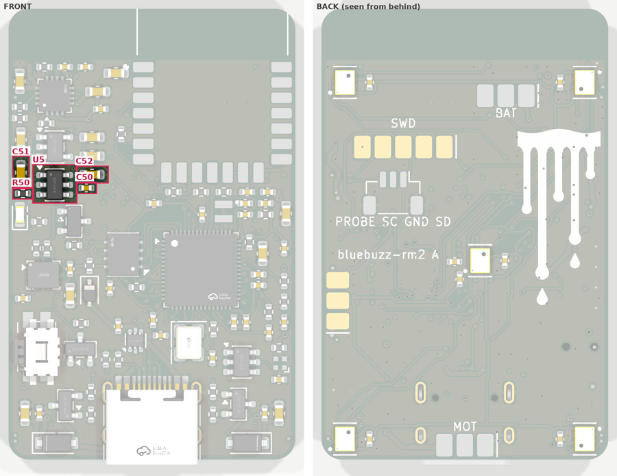
Schematic — block 5.Board — left side, below the LDO.
Datasheet —
the rise-time equation and table: 470 pF at 3.3 V gives 850 µs. TPS22918 p.14
Block 11Tactile array: five DPS368 barometers
Ref
Part
Value / MPN
LCSC
Why
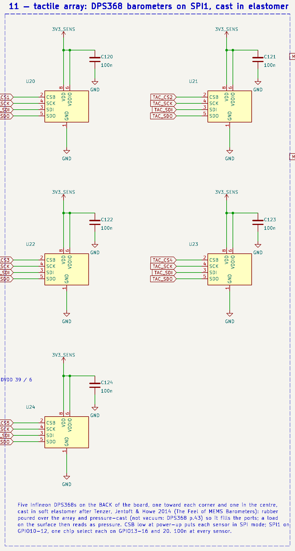
U20–U24
Barometer
Infineon DPS368XTSA1, LGA-8 2.0 × 2.5 × 1.1 mm
C3232508
Squeeze sensing after Tenzer, Jentoft and Howe
(2014): MEMS barometers cast under rubber read contact pressure. The DPS368 is small and waterproof (IPx8), with ±6 Pa relative accuracy and up to 128 Hz per sensor.
It speaks SPI. $4.21 each.
C120–C124
Decoupling
100 nF, one per sensor
C1525
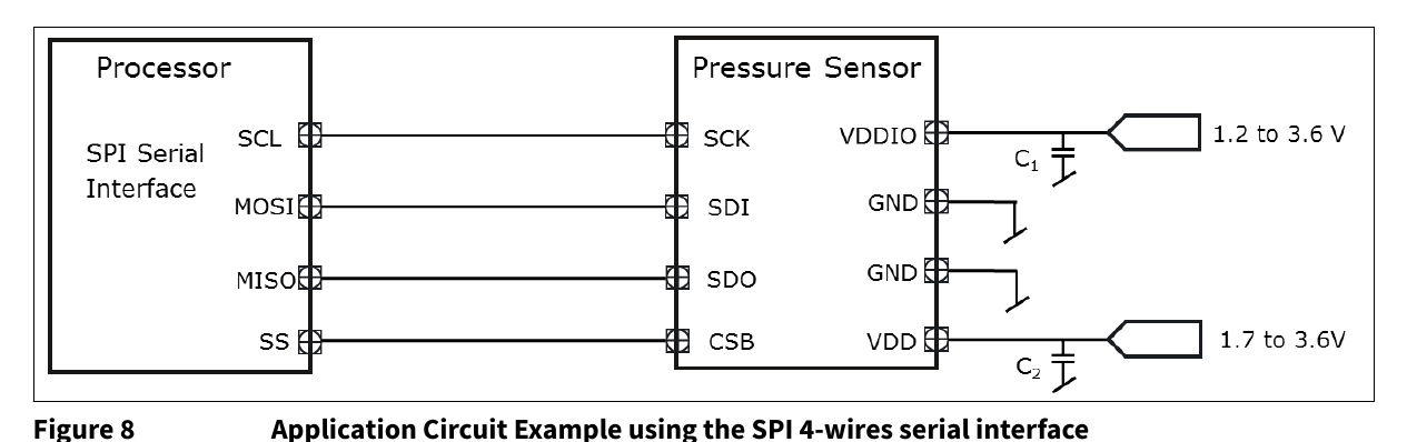
The datasheet shows 100 nF on each of VDD and VDDIO. Those pins are adjacent with GND between them and on
the same rail, so one cap within 1 mm of both serves them (a logged deviation).
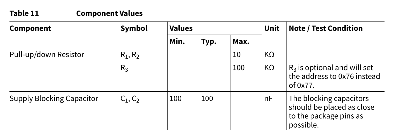
SPI with one chip select each (GPIO0, 14–16 and 20, mode 3, ≤ 10 MHz): the DPS368 has only two I2C addresses. The IMU stays on I2C so
that it is never an unpowered slave on a shared bus.
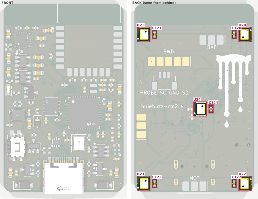
Positions: four corners plus the centre, all on the back facing the rubber. Each sits in a no-via area with its cap on the inboard side.
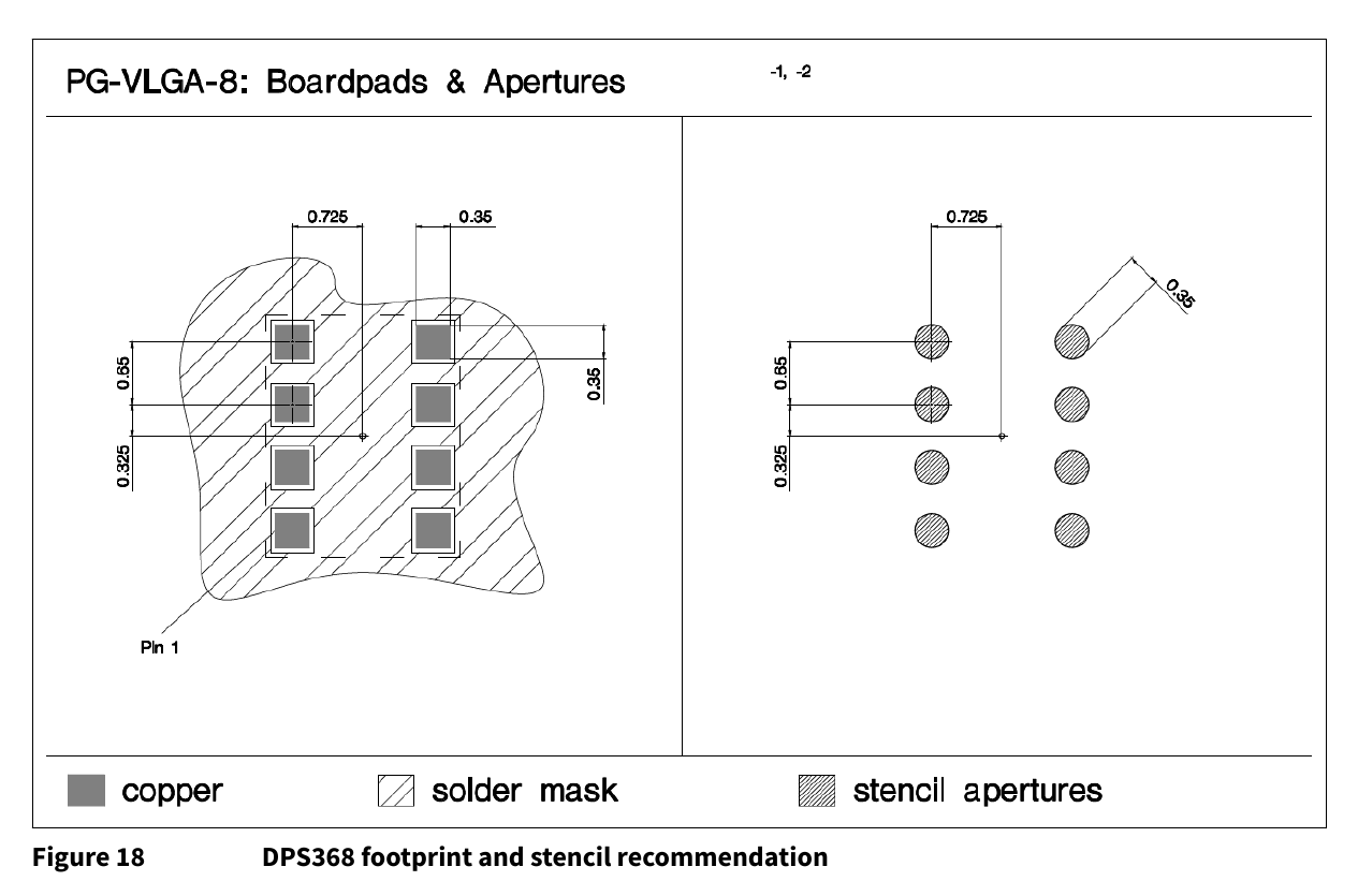
Land pattern: 0.35 × 0.35 mm solder-mask-defined pads with 0.35 mm paste, as in the datasheet's Fig. 18. The LCSC/EasyEDA land had 2.5 times the paste
on this 0.65 mm-pitch LGA, which cannot be reworked after casting.
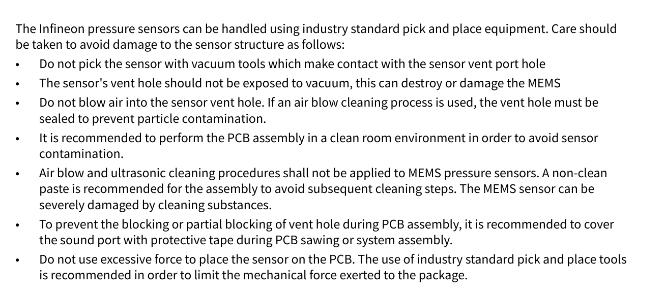
Casting: use a pressure pot or pre-degassed rubber, not vacuum over the board. The datasheet says the vent hole must not see vacuum.
Test one sensor in rubber first.
Firmware rule: hold all five CS lines high, raise SENS_EN, wait ≥ 12 ms, then pulse each CS low once (read ID 0x0D = 0x10). Until a
sensor sees CSB low it is an I2C slave at 0x77 on the shared SCK/SDI lines.
Schematic — block 11.Board — all on the back: four corners and the centre.
Datasheet —
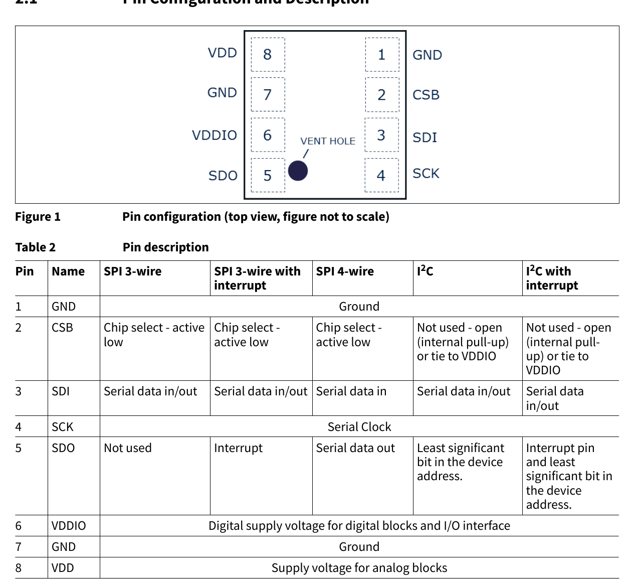
pinout and the SPI 4-wire pin roles. DPS368 p.6Datasheet —
the SPI 4-wire application circuit that this block follows. DPS368 p.19, Fig. 8Datasheet —
blocking caps, 100 nF "as close to the package pins as possible". DPS368 p.20, Table 11Datasheet —
the recommended pads and stencil the footprint now matches. DPS368 p.41, Fig. 18Datasheet —
handling: no vacuum on the vent hole, no blown air, no ultrasonic cleaning. DPS368 p.43
Block 12IMU
Ref
Part
Value / MPN
LCSC
Why
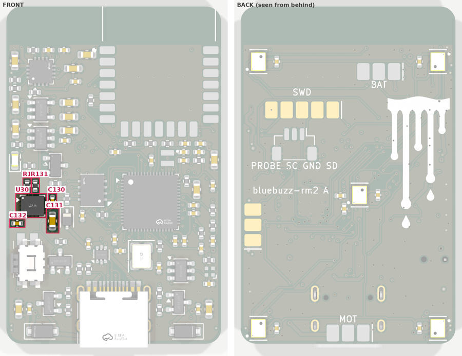
U30
6-axis IMU
ST LSM6DS3TR-C, LGA-14 2.5 × 3
C967633
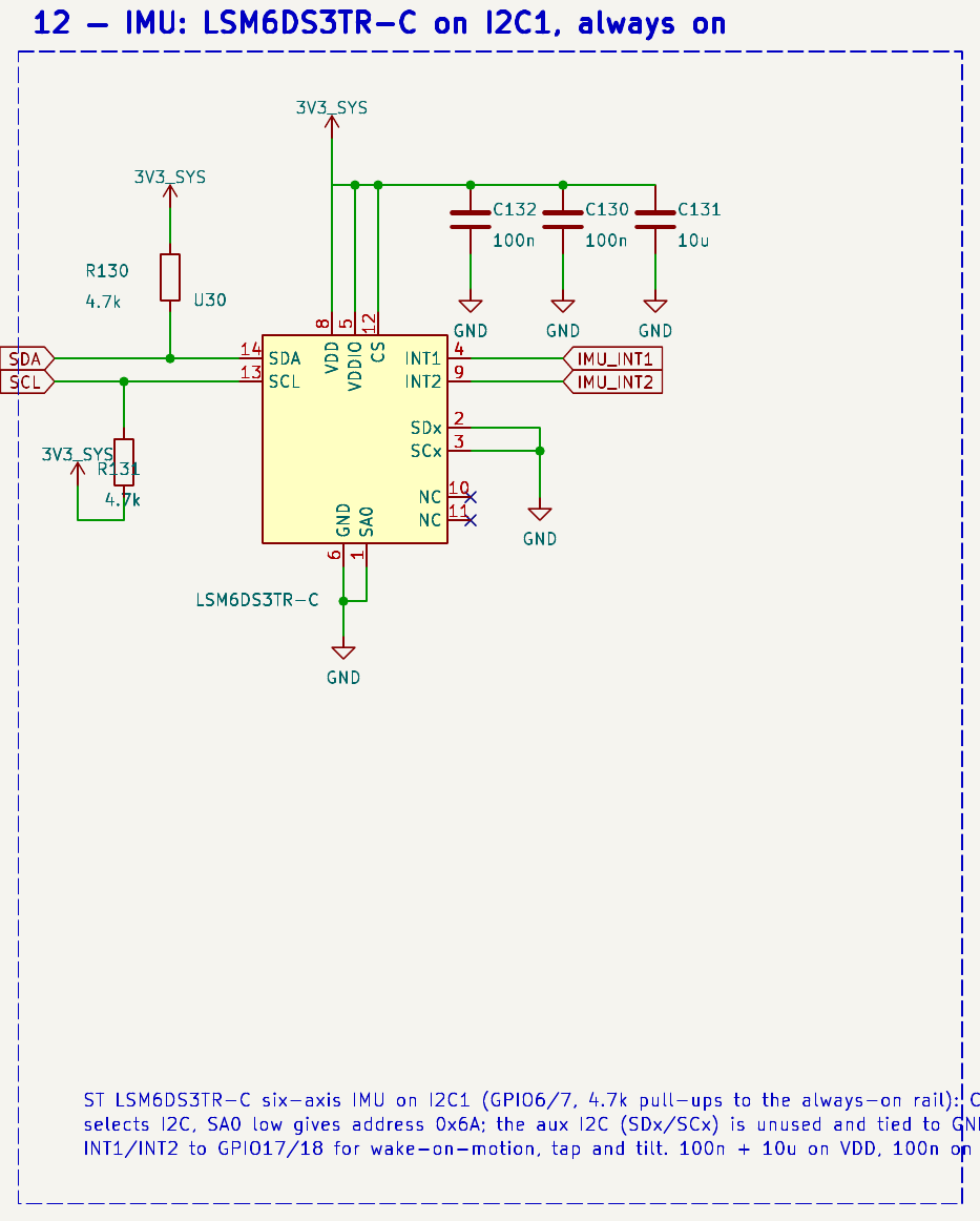
$1.67 with 14k in stock, against the BMI270 at $2.76 and the LSM6DSO at $3.90 with 519 in stock. Tap, wake-on-motion
and activity detection are built in. It runs on I2C1 at 0x6A (CS tied high, SA0 to GND), with INT1/INT2 on GPIO5/18.
R130, R131
I2C pull-ups
4.7 kΩ
C25900
Fast mode (400 kHz) up to about 75 pF of bus. The bus is a few cm with one device; the datasheet's example uses 10 kΩ.
C130, C132
VDD, VDDIO
100 nF each
C1525
One per supply pin, as the datasheet asks.
C131
Bulk
10 µF
C19702
Not required; included because the IMU shares 3V3 with the radio and the RP2350.
The aux-bus pins SDx/SCx (2, 3) are tied to GND. They are inputs with no pull, and the datasheet says "connect to VDDIO or GND".
Placed ≥ 1.5 mm in from the board edge, because package stress shifts the offsets. Calibrate the offsets after casting.
Motor vibration will trigger the wake and tap detectors while a motor runs, so firmware must ignore them during play.
Schematic — block 12.Board — left edge, middle, close to GPIO6/7.
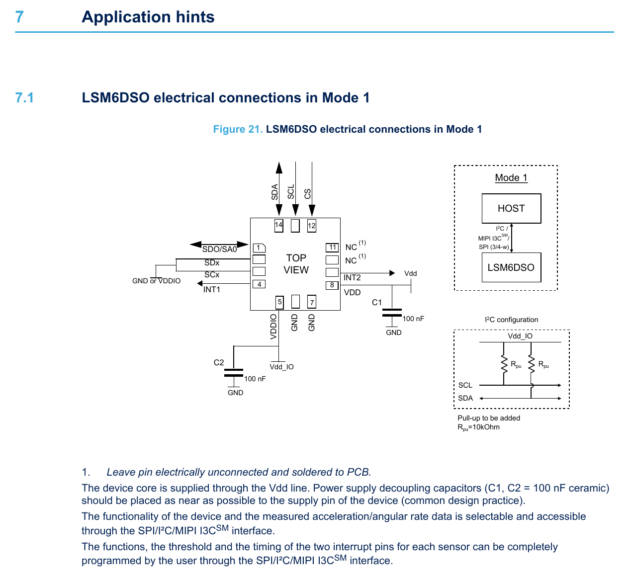
Datasheet (reference part) —
mode-1 connections of the LSM6DSO, which has the same package and pin positions. LSM6DSO p.35, Fig. 21
Datasheet missing: the LSM6DS3TR-C datasheet could not be downloaded (ST times out). Every number in its audit comes from
the LSM6DSO and is marked "verify". The register map and WHO_AM_I differ between the two parts, so firmware must use the DS3TR-C map. Please attach it.
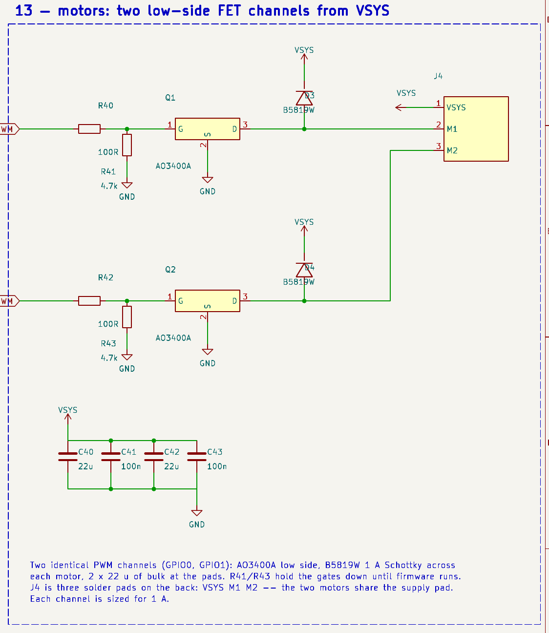
Block 13Motor channels
Ref
Part
Value / MPN
LCSC
Why
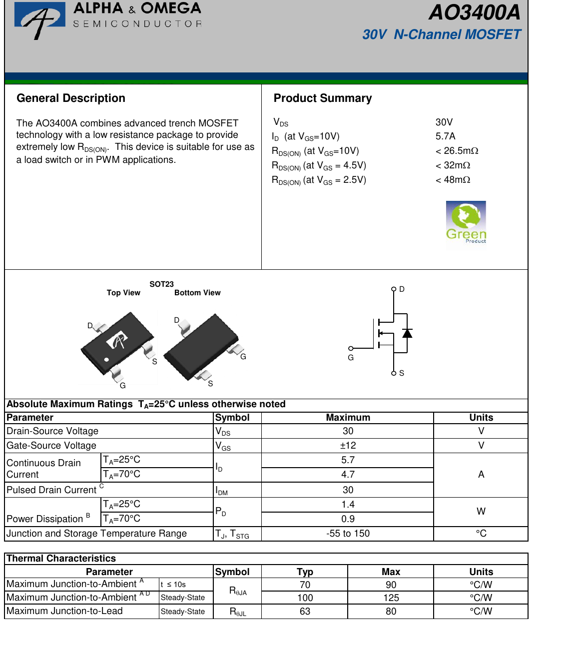
Q1, Q2
Low-side switch
AOS AO3400A, SOT-23
C20917
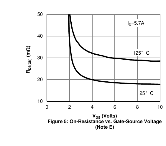
A JLC basic part. Logic level, 30 V, 5.7 A, with about 21 mΩ typ / 37 mΩ max at VGS = 3.3 V (Fig. 5).
At 0.2 A a channel dissipates about 1 mW, and even at the 1 A design figure only about 70 mW.
R40, R42
Gate series
100 Ω
C25076
Slows the edges to about 200 ns and damps ringing. The motor leads are antennas a few cm from the radio. That is 0.5 % of a 25 kHz period.
R41, R43
Gate pull-down
4.7 kΩ
C25900
Not 100 kΩ. RP2350 erratum E9: a GPIO configured as an input can leak about 120 µA and float near 2.2 V,
above VGS(th), which would run the motor uncontrolled at boot or in BOOTSEL mode. The erratum asks for ≤ 8.2 kΩ.
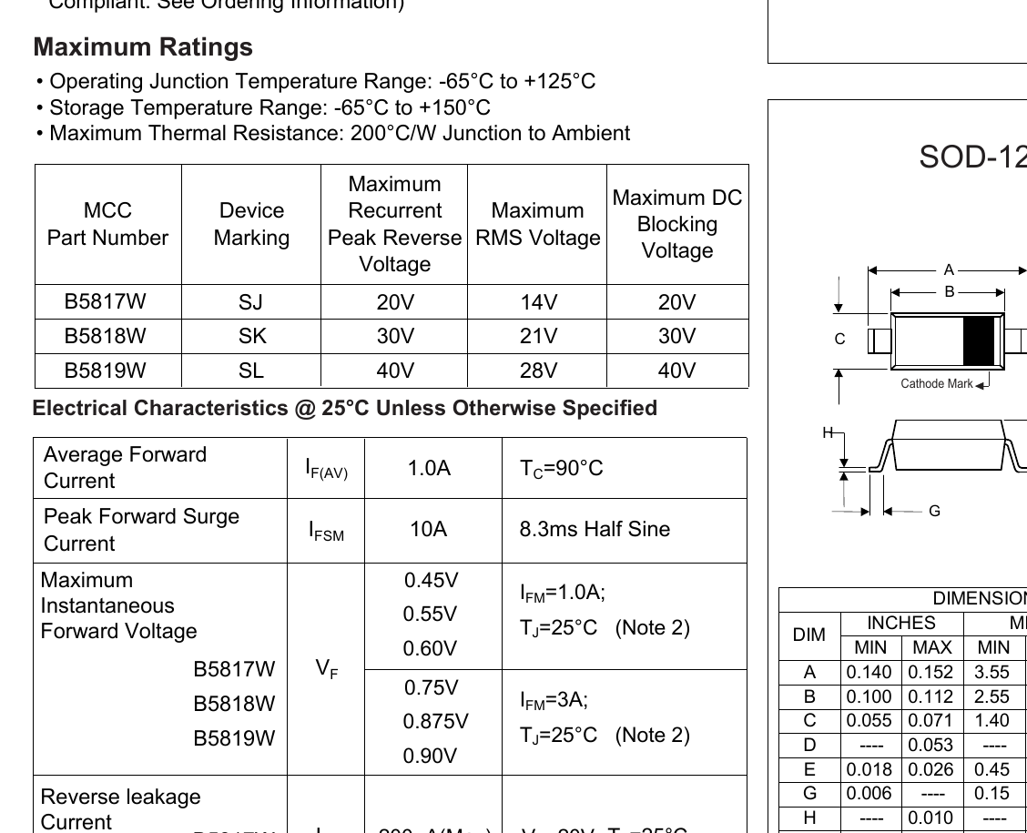
D3, D4
Flyback
B5819W, SOD-123 Schottky
C8598
1 A, 40 V, VF ≤ 0.6 V at 1 A. Clamps the switch node to VSYS when the FET turns off.
At 0.2 A it dissipates at most about 0.12 W (0.6 V × 0.2 A).
C40/C41, C42/C43
Bulk + HF
22 µF 0603 + 100 nF per channel
C86295, C1525
Supply the PWM current locally, so it does not pass through the cell lead
and the charger FET. VSYS ripple is about 0.1 V per channel at 0.2 A. Stagger the two PWM phases by 180° to halve it.
J4
MOT pads
3 pads, back: VSYS M1 M2
—
Each motor goes between VSYS and its Mn pad, and the FET sinks the current.
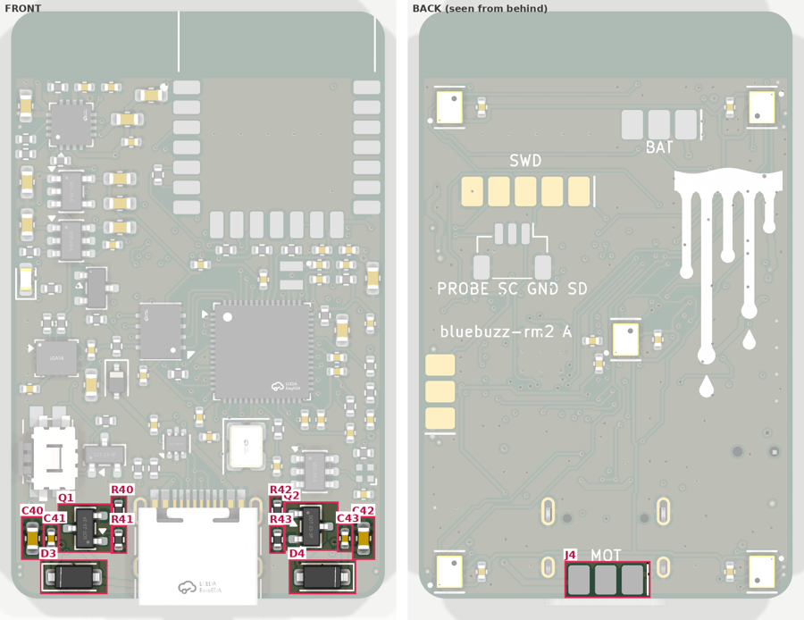
Schematic — block 13.Board — mirrored either side of the USB-C, each flyback in its corner;
the MOT pads are on the back between the receptacle's shell pads.
Datasheet —
AO3400A ratings: VDS 30 V, VGS ±12 V, RDS(on) < 48 mΩ at 2.5 V. AO3400A p.1Datasheet —
RDS(on) against VGS: about 21 mΩ at the 3.3 V drive. AO3400A p.3, Fig. 5Datasheet —
B5819W: 40 V, 1 A, VF 0.6 V at 1 A, Tj ≤ 125 °C. This is MCC's sheet; the LCSC part may come from another maker with the same ratings. B5817W–B5819W p.1
Block 6Debug and test pads
Ref
Part
Value / MPN
LCSC
Why
J3
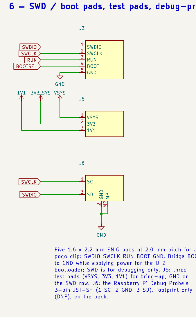
SWD pogo row
5 pads, back: SWDIO SWCLK RUN BOOT GND
—
Program and debug before casting with a pogo clip; ENIG finish, no paste. BOOT bridged to GND at power-up
gives the UF2 bootloader. Placed on the back under the radio, where nothing else lands.
J5
Test pads
3 pads, back: VSYS 3V3 1V1
—
The three rails a first power-up checks. 1V1 under load is also the acceptance test for the core inductor.
J6
Debug Probe connector
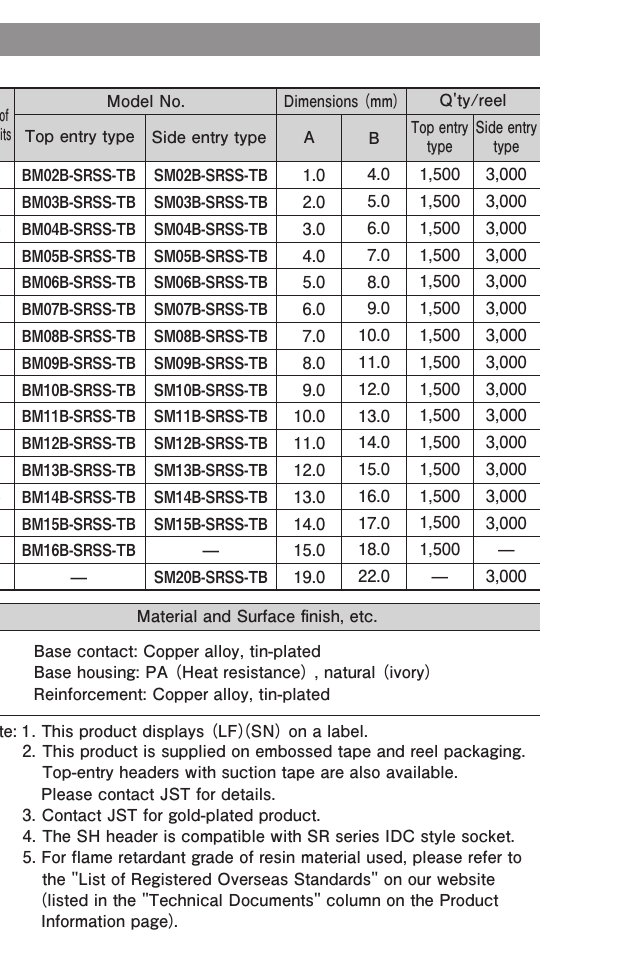
JST SH BM03B-SRSS-TB, not fitted
(C160389)
Footprint for the Raspberry Pi Debug Probe's 3-pin
cable, in its order SC, GND, SD. It is hand-fitted for bench work and left out of the BOM and CPL.
Schematic — block 6.Board — back, under the radio.
Datasheet —
SH headers: BM03B-SRSS-TB is the 3-circuit top-entry part. JST SH p.3
Passives
Sizes: 0402 throughout. 0603 is used for 1 µF (to get a 50 V X5R that keeps its capacitance at 4.4 V) and for 10 µF and 22 µF, which a 10 V
0402 cannot give usefully after DC bias. 4.7 µF on the RP2350 rails is a 0402 X5R 10 V, as in the reference design.
Dielectrics: X7R 16 V for 100 nF. C0G for the crystal loads (15 pF) and the CT timing cap (470 pF), whose values must not drift with voltage.
DC bias is accounted for in each audit. The 10 µF 0603 10 V parts are about 7 µF at 3.3–4.4 V, and the 22 µF about 9–12 µF at 4.4 V.
JLC basic parts wherever a choice allowed (C1525, C15849, C19702, C23733, most 0402 resistors). The 27 Ω, the charger's set resistors
and the 22 µF are extended parts, accepted for the values the datasheets ask for.
Placement: every passive sits at the pin it serves, on the same side as its chip. The exceptions are C81, C91, C97 and C98 behind the RP2350, and
the sensors' caps on the back.
missing (low risk: basic parts or the reference design's own)
Open items that touch component choices
Cell: ≥ 700 mAh, with its own protection PCB. If it has a 10 k NTC, wire it to T and leave R13 off. Set R12 for the capacity if the 6 h timer is too short.
Inductor orientation: at assembly, confirm the Abracon dot is on pad 1 as in Raspberry Pi's layout.
Casting tests: cast one DPS368 in rubber first (pressure pot, no vacuum), and measure RM2 range in air and when cast.
Firmware contracts that the parts depend on: drive GPIO19 high early; cut off at a 3.5 V cell; follow the DPS368 CS order; park the SPI lines before cutting the
sensor rail; enable the GPIO9 pull-up; set GPIO13/17 to 12 mA drive; stagger the motor PWM; calibrate the IMU after casting; use the LSM6DS3TR-C register map.
Datasheets to attach: LSM6DS3TR-C, USBLC6-2, TYPE-C-31-M-12 (see above).
Full component list
Generated from circuit.py and bom/parts.yaml by scripts/doc_images.py
(parts.json). Click a block number to jump to its section.